


研究半导体器件材料去除行为的方法,有分子动力学法和纳米划痕实验法[14~25]。但是,纳米划痕实验法不能描述原子尺度划痕材料去除的动态微结构演化和观察其内部相变转化过程,而分子动力学法可模拟上百万原子体系和精准描述材料去除信息。进行微划痕测试可研究材料的抗划伤性[14, 15]、多层涂层结构完整性[16]、摩擦学行为[17, 18]和接触损伤[19]。Meng等[20]进行Berkovich压头纳米划痕实验研究了6H-SiC单晶的去除机理,发现实验测得的塑性-脆性转变临界切削深度约为用经验公式计算结果的5倍[21]。用透射电镜观察到,划痕底部下表面附近的非晶态相和位错可触发材料的塑性去除。研究发现[22],进行微划痕测试,可了解材料的特性、尖端的几何形状以及压头与试样界面处的应力分布对加工深度的影响。4H-SiC沿1120方向的划痕更容易产生裂纹扩展,沿1010方向的加工表面质量较好。Tian等[23]在(0001)晶面(即Si平面)上对4H-SiC和6H-SiC纳米压痕的分子动力学模拟表明,由内部滑移引起的非晶结构有沿[1120]方向扩展的趋势。对3C-SiC单晶纳米压痕的MD模拟表明,棱柱位错环是由两个独立的位错环交叉滑移形成的[24]。Tian等[25]模拟了4H-SiC和6H-SiC的刮擦,发现C平面的材料去除比Si平面更有效,且非晶的变形更小。Wang和Fang[26]对单晶6H-SiC超精密切削加工发现,加工表面的亚表层产生了纳米级裂缝,裂纹的扩展方向发生突变。田东禹[27]研究了单晶3C-SiC在单点金刚石刀具切削作用下的切削机制。结果表明,进行延性域切削时非晶层的厚度随着切削深度的增加而增加;发生脆塑转变后,随着切削深度的增加非晶层厚度逐渐减小最后消失。Zhou等[28]研究了含空位缺陷的单晶SiC衬底的去除机理和金刚石磨料的磨损机理。结果表明,在SiC衬底上出现了更多的空位缺陷,从而提高了去除效率和减少了亚表面损伤。
目前对SiC的研究集中在划痕损伤行为、超精密加工、材料去除行为。本文对β-SiC半导体器件在滑动摩擦中的材料去除行为进行纳观分析。
1 理论计算方案和参数
1.1 条件的设置
图1给出了β-SiC滑动摩擦的三维原子尺度物理模型,采用的磨粒形状为虚拟球。β-SiC模型的尺寸为Lx = 28.3 nm、Ly = 46.8 nm、Lz = 26.3 nm (图1a)。模型X、Y、Z的晶向分别为[
图1
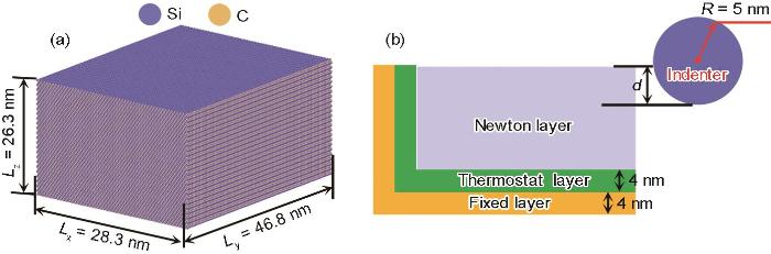
图1
β-SiC纳米滑动摩擦三维分子动力学模型
Fig.1
Three dimensional model of β-SiC constructed by molecular dynamics method (a) β-SiC atomic model, (b) schematic diagram of sliding friction
表1 β-SiC纳米滑动摩擦参数设置
Table 1
| Simulation condition | Parameters setting |
|---|---|
| Model dimension (L) | Lx (28.3 nm) × Ly (46.8 nm) ×Lz (26.3 nm) |
| Cutting speed (V) | 100 m/s, 200 m/s, 300 m/s |
| Cutting depth (d) | 3 nm, 5 nm, 7 nm |
| Abrasive particle radius (R) | 5 nm, 7 nm, 9 nm |
| Newton layer (T) | 1 K, 300 K, 800 K |
| Crystal plane | (001), (110), (111) |
| Time step | 1 fs |
1.2 势函数
为了准确描述SiC内部结构受接触载荷产生的亚表层损伤,用Vashishta势函数描述SiC受载产生的位错和相变[30]。总能量为
式中,
1.3 应力和应变
用维里应力
描述材料塑性变形程度,用剪切应变
描述接触区应变度[31]。
2 结果和讨论
2.1 切向力与剪切变形
图2a~d给出了磨粒半径、压深、服役温度、晶面选择性对β-SiC滑动磨损水平切向力的影响。可以看出,在滑动5 nm前β-SiC以受载产生的晶格挤压为主,磨损量很小。水平切向力与滑动距离呈线性关系:随着滑动距离的增加水平切向力逐渐增大。这个关系,受磨粒半径、压深、服役温度、晶面选择性改变的影响很小。滑动距离超过5 nm则水平切向力的稳定性较高。此阶段的滑动磨损材料去除处于塑性变形稳定期,波动幅度较小。水平切向力与滑动摩擦变量改变的关系为:随着磨粒半径的增大水平切向力逐渐增大,随着压深的增大水平切向力随之增大;随着服役温度的提高水平切向力减弱;β-SiC不同的晶面,其水平切向力也有所不同(图2e)。图2e~h给出了图2a~d中滑动5 nm后对应的平均摩擦力与滑动摩擦变量的关系。可以看出,磨粒半径、压深、服役温度、晶面选择性显著改变了磨损稳定阶段的平均摩擦力。磨粒半径从5 nm增加到9 nm时平均摩擦力增大了5.9倍;磨粒压深从3 nm增加到7 nm平均摩擦力增大了3.16倍;服役温度从T = 1 K提高到800 K平均摩擦力减小,下降幅度为12.85%;β-SiC的晶面中(001)面的平均摩擦力最大,其次是(110)面,(111)面的最弱。
图2
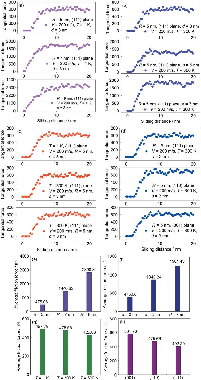
图2
滑动摩擦参数对β-SiC平均摩擦力影响
Fig.2
Influence of sliding friction parameters on friction force (a-d) and average friction force (e-h) for β-SiC material (a, e) effect of abrasive particle radius on friction force, (b, f) effect of indentation depth on friction force, (c, g) effect of temperature on friction force, (d, h) effect of crystal plane on friction force
图3a~c给出了服役温度从低温提高到高温β-SiC纳米滑动摩擦中原子的迁移幅度和剪切变形。从图3a可见,磨损产生的磨屑原子堆积在磨粒的正前方和接触边缘两侧,且在接触边缘两侧磨损原子的分布较为均匀。同时,随着服役温度的提高磨粒正前方和接触边缘两侧堆积的磨损原子增多。其主要原因是,温度的升高弱化了碳硅的结合键能,使磨损更易发生。在β-SiC的端部,在以弹性期为主的磨损过程和稳定期磨损阶段,原子的位移幅度随着温度的升高而加剧。从图3b可见,磨粒与β-SiC紧密接触区外侧的原子位移幅度由上向下呈递减趋势,并随着服役温度的升高而加剧(图3b中的紫色箭头)。图3c表明,随着服役温度的升高剪切变形的规律与图3b中原子位移幅度的分布趋势一致。图4a~c给出了滑动速度从100 m/s提高到300 m/s对β-SiC纳米滑动磨损阶段的原子迁移幅度和剪切变形的影响。从图4a、b可见,随着滑动速度的提高磨粒正前方和接触边缘两侧堆积的磨损原子减少。同时,在β-SiC端部和接触区外侧的原子其位移幅度和滑动速度的提高尚未出现单调递增或递减的趋势。从图4c可见,在β-SiC接触区两侧剪切变形最严重,挤压出的磨屑原子堆积在边缘两侧,分布规律与原子位移幅度一致。图5给出了不同晶面和压深对β-SiC纳米滑动磨损的原子位移幅度影响。从图5a~e可见,晶面选择性和压深显著影响原子的位移幅度,表现为接触边缘两侧挤出的磨损原子分布不均,接触区外侧的位移幅度由内到外逐渐衰减(图5a1~e1)。不同晶面中(111)面接触区外侧的位移幅度最大,其次是(110)面,最后才是(001)面。
图3
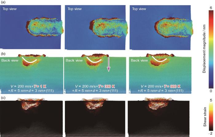
图3
温度对β-SiC纳米滑动磨损的原子位移幅度和剪切变形影响
Fig.3
Influence of temperature on atomic displacement amplitude and shear deformation of β-SiC under nano-sliding wear (a) effect of temperature on atomic displacement amplitude from top view, (b) effect of temperature on atomic displacement amplitude from back view, (c) effect of temperature on shear strain from back view
图4

图4
滑动速度对β-SiC纳米磨损阶段的原子位移幅度和剪切变形的影响
Fig.4
Influence of sliding velocity on atomic displacement amplitude and shear deformation of β-SiC under nano-wear stage (a) effect of sliding speed on atomic displacement amplitude from top view, (b) effect of sliding speed on atomic displacement amplitude from back view, (c) effect of sliding speed on shear strain from back view
图5

图5
晶面选择性和压深对β-SiC纳米滑动磨损的原子位移幅度影响
Fig.5
Influence of crystal plane selectivity and indentation depth on atomic displacement amplitude of β-SiC under nanosliding wear (a-e) effect of crystal plane and indentation depth on atomic displacement amplitude from top view, (a1-e1) effect of crystal plane and indentation depth on atomic displacement amplitude from back view
2.2 微结构的演化
图6给出了温度、速度、压深和晶面对β-SiC滑动摩擦中微结构演化的影响。可以看出,β-SiC在纳米磨损的塑性变形中塑性环脱落。脱落前,塑性环经历了形核、生长和繁衍,且β-SiC的塑性变形以Shockley不全位错和立方晶体结构向闪锌矿晶体结构相变转化为主。在滑动磨损中,磨粒和基底挤压区因受载而产生高应力。应力超过临界分解剪切应力值时位错形核并增殖,位错通过耦合反应和滑移释放应力。随着滑动距离的增加挤压区的应力累积并伴随着Shockley不全位错的生成和滑移。一个全位错可用两个相邻的Shockley不全位错表示,其关系为
图6
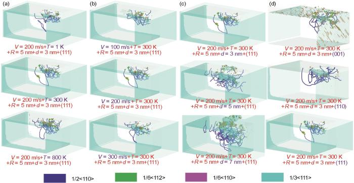
图6
滑动摩擦参数对β-SiC微结构演化影响
Fig.6
Influence of sliding friction parameters on the microstructure evolution of β-SiC (a) effect of temperature on microstructure evolution, (b) effect of sliding speed on microstructure evolution, (c) effect of indentation depth on microstructure evolution, (d) effect of crystal plane on microstructure evolution
2.3 材料去除的机理
图7给出了温度、速度、压深和磨粒半径对β-SiC原子矢量位移的影响。从图7可见,磨屑原子的矢量位移最大,表层及以下的原子在水平摩擦力的诱导下其矢量位移逐渐减弱。同时,β-SiC端部原子的矢量位移出现与磨粒运动方向相反的回流运动趋势。其主要原因是,表层摩擦产生的较高温度导致原子热运动迁移。随着服役温度的提高和压深的增大摩擦过程中β-SiC的原子矢量位移逐渐减弱;随着滑动速度的提高β-SiC的原子矢量位移逐渐增大。图8a~d给出了滑动摩擦参数对β-SiC的磨屑原子的具体量化比较。图8e定性地给出了滑动参数对磨屑原子数的影响。从图8可见,随着滑动距离的增加磨屑原子数递增而呈现出抛物线增长趋势。随着压深的增大和温度的提高,磨屑原子数逐渐增加。但是,随着滑动速度的提高磨屑原子数逐渐下降。β-SiC的晶面选择性对磨屑原子数的产生也有显著的差异:在(001)面产生磨屑的原子最多,其次(110)面,最少是(111)面。其主要原因是,(001)面的水平切向力最大,(111)面的水平切向力最小。
图7

图7
滑动摩擦参数对β-SiC原子矢量位移的影响
Fig.7
Influence of sliding friction parameters on the vector displacement of β-SiC atoms (a-c) the influence of sliding speed and abrasive radius on the vector displacement of β-SiC, (d-f) the influence of temperature on the vector displacement of β-SiC, (g, h) the influence of sliding speed and indentation depth on the vector displacement of β-SiC
图8
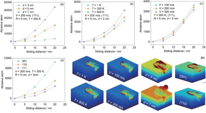
图8
滑动摩擦参数对β-SiC磨屑原子数的影响
Fig.8
Influence of sliding friction parameters on the atomic number of β-SiC with grinding chips (a) the influence of indentation depth on abrasive atoms, (b) the influence of temperature on abrasive atoms, (c) the influence of sliding speed on abrasive atoms, (d) the influence of crystal plane on abrasive atoms, (e) influence of sliding friction parameters on abrasive atoms
为了定量比较β-SiC滑动磨损过程的表面非晶原子数随摩擦参数的变化,图9给出了各摩擦参数的改变对β-SiC摩擦的径向分布函数的影响。径向分布函数描述了以给定的一个粒子作为参考点其他粒子在邻域空间中的分布概率,其峰值可表示为基底受载产生的非晶化程度[32]。从图9可见,随着磨粒半径、压深的增加和滑动速度的提高径向分布函数的峰值增大。这表明,在β-SiC的滑动磨损过程中产生的表面非晶原子数逐渐增多。但是,随着服役温度的提高径向分布函数的峰值减小,表明在β-SiC的滑动磨损过程中产生的表面非晶原子数逐渐减少。其主要原因可能是,温度的提高使原子间键合力减小和空位增加,在β-SiC基底内更易产生各类型的位错,从而减少了表面非晶原子数。为了深入了解磨屑的形成机理和材料去除机制,图10和11分别给出了β-SiC在滑动磨损过程中的应力场和温度场分布,以及滑动摩擦参数的变化。从图10可见,水平摩擦力的诱导使β-SiC的Von Mises应力主要分布在磨粒与基底的挤压区和亚表层,尤其以挤压区的高应力为主,从而破坏了β-SiC的碳与硅键能结合,产生的磨屑原子堆积在磨粒的正前方和接触区边缘两侧。同时,β-SiC的应力场分布区域的集中程度与图6给出的β-SiC基底内位错的形核、生长、繁殖区域形成的趋势一致,即β-SiC基底产生的位错越多Von Mises应力就越集中于该区域。此外,随着温度的升高β-SiC的挤压区应力更加集中,也是温度上升磨屑原子数增多的内在原因。随着滑动速度的提高和压深的增加,β-SiC的挤压区应力分布也更加集中。β-SiC的应力分布还与晶面选择性有密切的关系。为了更好地了解β-SiC材料磨损的去除机制,图11给出了摩擦参数对磨损过程中温度场分布的影响。从图11可见,β-SiC的已滑动表面和磨屑原子堆积处的温度场分布最高。在同等条件下滑动速度越高和压深越大,越容易导致挤压区和磨粒与β-SiC紧密接触区边缘和被刮擦后的表面温度升高,从而提高基底表面去除材料的流动性(图7),使底部接触区的磨屑原子更容易凝聚成粘着结点,与图11中对应的摩擦参数改变对温度场分布的影响和图10中的Von Mises应力分布特征有良好的一致性。图10和图11中的Von Mises应力分布和温度场分布表明,β-SiC滑动磨损中材料去除的主要原因,是挤压区的高应力和高温度,使材料在水平摩擦力的诱导下更容易从材料表面去除而形成磨屑原子。
图9
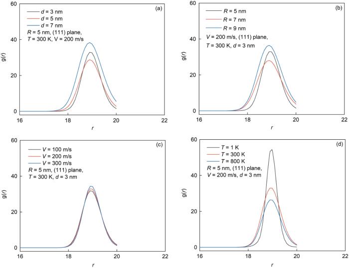
图9
滑动摩擦参数对β-SiC径向分布函数影响
Fig.9
Influence of sliding friction parameters on the radial distribution function of β-SiC (a) indentation depth effect, (b) particle radius effect, (c) sliding speed effect, (d) temperature effect
图10
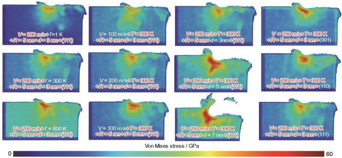
图10
滑动摩擦参数(温度、速度、压深、晶面)对β-SiC应力场分布的影响
Fig.10
Influence of sliding friction parameters for temperature, velocity, indentation depth and crystal plane on the stress field distribution of β-SiC
图11
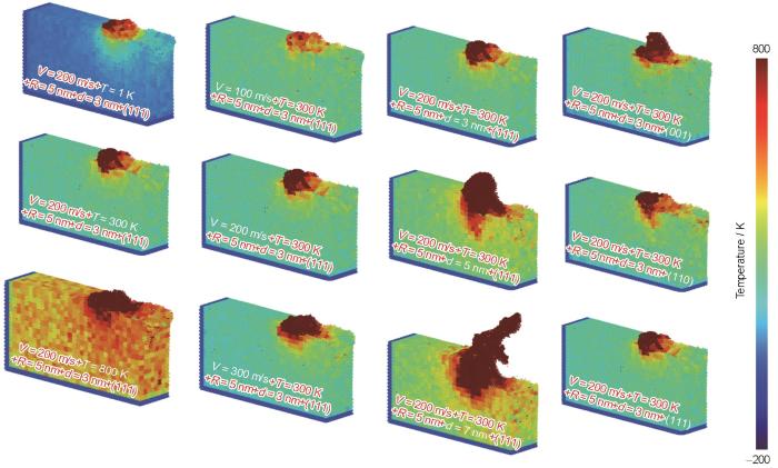
图11
滑动摩擦参数(温度、速度、压深、晶面)对β-SiC温度场分布的影响
Fig.11
Influence of sliding friction parameters for temperature, speed, indentation depth and crystal plane on the temperature field distribution of β-SiC
3 结论
(1) 在滑动摩擦初期,β-SiC的水平切向力与滑动距离呈线性关系,在随后的摩擦稳定期水平切向力呈现波动幅度较小的稳定趋势。磨粒半径、压深、晶面选择性、服役温度显著改变了磨损稳定阶段的平均摩擦力。
(2) 随着服役温度的升高碳与硅的结合键能弱化,磨粒正前方和接触边缘两侧堆积的磨损原子增多,磨损更易发生。随着滑动速度的提高磨粒正前方和接触边缘两侧堆积的磨损原子减少。晶面选择性和压深显著影响原子位移幅度,即接触边缘两侧挤出的磨损原子分布不均,接触区外侧的位移幅度由内到外呈衰减趋势。
(3) 随着服役温度的提高和压深的增加,Shockley不全位错的高速生长、增殖和滑移也随之显著。随着滑动速度的提高Shockley不全位错的高速生长、增殖、滑移减弱。
(4) 在β-SiC纳米滑动磨损中材料的去除机制是,磨粒与β-SiC挤压区强烈的高温高应力分布导致β-SiC更易受水平摩擦力诱导而从表面去除,形成磨屑原子堆积在磨粒正前方和接触区边缘两侧。在同等条件下,滑动速度越高和压深越大,越容易导致挤压区和磨粒与β-SiC紧密接触区边缘两侧和刮擦后的表面温度升高,加速基底材料的去除。
参考文献
Wide band gap a-SiC:H films for optoelectronic applications
[J]. J.
Evaluation of switching loss contributed by parasitic ringing for fast switching wide band-gap devices
[J].
Demonstration and analysis of a 600 V, 10 A, 4H-SiC lateral single RESURF MOSFET for power ICs applications
[J].
Dislocations in 4H-and 3C-SiC single crystals in the brittle regime
[J].
Determination of the electric field in 4H/3C/4H-SiC quantum wells due to spontaneous polarization in the 4H SiC matrix
[J].
Electrical impact of SiC structural crystal defects on high electric field devices
[J].
The effect of an electric field on self-sustaining combustion synthesis: Part II. field-assisted synthesis of μ-SiC
[J].
Static dielectric constant of SiC
[J].
Electrical instability of low-dielectric constant diffusion barrier film (a-SiC:H) for copper interconnect
[J].
Modeling and simulation in tribology across scales: an overview
[J].
Depth-dependent hysteresis in adhesive elastic contacts at large surface roughness
[J].
Contact force-indentation depth measurements in contact experiments involving compliant materials, such as polymers and gels, show a hysteresis loop whose size depends on the maximum indentation depth. This depth-dependent hysteresis (DDH) is not explained by classical contact mechanics theories and was believed to be due to effects such as material viscoelasticity, plasticity, surface polymer interdigitation, and moisture. It has been observed that the DDH energy loss initially increases and then decreases with roughness. A mechanics model based on the occurrence of adhesion and roughness related small-scale instabilities was presented by one of the authors for explaining DDH. However, that model only applies in the regime of infinitesimally small surface roughness, and consequently it does not capture the decrease in energy loss with surface roughness at the large roughness regime. We present a new mechanics model that applies in the regime of large surface roughness based on the Maugis-Dugdale theory of adhesive elastic contacts and Nayak's theory of rough surfaces. The model captures the trend of decreasing energy loss with increasing roughness. It also captures the experimentally observed dependencies of energy loss on the maximum indentation depth, and material and surface properties.
Fracture mechanics analysis of asperity cracking due to adhesive normal contact
[J].
Effects of normal load on the coefficient of friction by microscratch test of copper with a spherical indenter
[J].
Rate and load effects on scratch behavior of thermoplastics by berkovich indenter
[J].
Adhesion analysis of polycrystalline diamond films on molybdenum by means of scratch, indentation and sand abrasion testing
[J].
Influence of poly(ethyleneimine) functionalized multi-walled carbon nanotubes on mechanical and tribological behavior of epoxy resins
[J].
Investigating the effects of microstructure on the wear mechanisms in lamellar cast irons via microscratch tests
[J].
Sliding of a diamond sphere on fused silica under ramping load
[J].
Material removal mechanism of 6H-SiC studied by nano-scratching with Berkovich indenter
[J].
Ductile-regime grinding: a new technology for machining brittle materials
[J].
Investigation of the anisotropy of 4H-SiC materials in nanoindentation and scratch experiments
[J].
Study on nanomechanical properties of 4H-SiC and 6H-SiC by molecular dynamics simulations
[J].
Molecular dynamics simulation in single crystal 3C-SiC under nanoindentation: formation of prismatic loops
[J].
Molecular dynamics simulation of the material removal in the scratching of 4H-SiC and 6H-SiC substrates
[J].
Nanometric cutting mechanism of silicon carbide
[J].
Research on 3C-SiC nanometric cutting mechanism under SEM online observation
[D].
3C-SiC的SEM在线纳米切削机理研究
[D].
Atomic-scale study of vacancy defects in SiC affecting on removal mechanisms during nano-abrasion process
[J].
Fast parallel algorithms for short-range molecular dynamics
[J].
Atomic analysis of contact-induced subsurface damage behavior of single crystal SiC based on molecular simulation
[J].It is helpful to understand the microstructure evolution characteristics and mechanical properties of monocrystalline SiC semiconductor devices during contact from the perspective of atomic scale to understand the microscopic mechanism of subsurface damage behavior and phase transformation. Based on the Vashishta potential function of molecular dynamics, the microscopic evolution characteristics of the nano-indentation induced dislocation rings, the amount of phase transformation and the contact mechanical properties of the corresponding monocrystalline SiC surface were studied, and the effect of extreme service temperature on the subsurface damage behavior and the contact mechanical properties were analyzed. The results show that the plastic deformation of SiC subsurface damage is mainly caused by dislocation nucleation, dislocation accumulation and dislocation slip, whilst the dislocation ring goes through four evolution stages during contact, i.e., dislocation nucleation, dislocation ring growth, dislocation ring reproduction and dislocation ring brittle break. Besides, with the increasing temperature, the maximum bearing capacity, hardness, Young's modulus and contact stiffness curves of silicon carbide materials show a parabolic trend of decline. The main reason is that the higher the temperature is, the SiC lattice is easy to get rid of the bondage of atomic bond energy, resulting in lattice defects, and easy to breed dislocation, which result in the enrichment of stress concentration on subsurface of materials at lastly. As a result, the mechanical properties of SiC materials are greatly reduced while being contacted. In addition, the subsurface stress concentration is also the fundamental reason for the phase transformation from cubic to sphalerite for SiC materials. With the increase of temperature, the amount of phase transformation increases. The dynamic contact plastic deformation and micro-structure evolution of SiC in semiconductor devices under loading, and the phase transformation are significantly dependent on the operating temperature. The rising temperature related change of crystal lattice and the generation of random rough spots on the surface are the main causes of contact adhesion. This study may provide a deeper understand on contact mechanical properties and sub-surface damage behavior at extreme service temperatures, and will also enrich the understanding of the contact failure mechanism of nano silicon carbide.
单晶碳化硅接触中亚表层损伤与破坏机理的原子尺度分析
[J].
Temperature effect on mechanical response of c-plane monocrystalline gallium nitride in nanoindentation: a molecular dynamics study
[J].
