


李晓伟等[8]计算了掺杂不同种类和含量的金属时非晶碳的电子结构,发现掺入过渡金属可降低这个体系的总畸变能量从而降低残余应力,掺杂Cu,可使其具有Cu-C反键态特征。Yaremchuk等[9]用磁控溅射技术沉积了不同Cu含量的a-C: H: Cu薄膜,发现掺杂Cu的非晶碳具有等离子体共振效应,共振吸收峰的位置向短波方向移动。Beauty等[10]用电化学沉积制备了不同Ni含量的非晶碳薄膜,随着Ni含量的降低,这种薄膜的光学带隙逐渐下降。Meskinis等[11]用反应磁控溅射制备Ni掺杂非晶碳新型敏感材料,研究了Ni掺杂对其电学和压阻性能的影响。结果表明,改变掺入Ni的含量可大范围调控非晶碳的电阻率,Ni含量低于4%(原子分数)的样品,其压阻系数大于3000,远比纯非晶碳和常用Si材料的高。
与晶体半导体不同,非晶半导体中既有扩展态又有定域态,而定域态电子只能通过隧穿或者热激活方式传导[12]。非晶碳中的碳原子主要以sp2和sp3杂化的形式存在,sp2杂化碳既有σ键又有π键。位于费米能级附近的π电子决定非晶碳的电学特性[13],而π键又与原子间距和配位数密切相关。非晶碳复杂的键态结构,使其载流子输运机理的研究进展缓慢。Tripathi等[14]指出,纯非晶碳的载流子输运方式为Mott型变程跳跃传导。Abdolghaderi等[15]调控非晶碳中Ag的掺入量使载流子输运方式变为渗流特性。万蔡华等[16]发现,在非晶碳中掺入Fe使载流子的输运方式从低温到高温依次从Efros-Shklovskii(ES)型变为跳跃传导(<60 K)、Mott型三维变程跳跃传导(60~200 K)或热激活传导(>200 K)。掺杂多种金属与碳成键的特征差异较大[17,18],金属能以固溶或以金属和碳化物纳米晶的形式存在于非晶碳基质中[7]。同时,随着金属含量的变化非晶碳的结构和载流子输运行为极为复杂。载流子的输运机理不明确,限制了碳基薄膜光电器件的设计和应用。
在非晶碳中掺入Cu使C 2p轨道与Cu 3d轨道杂化,电子占据能量较高的反键态,即Cu和C成反键特征[8]。这表明,a-C: Cu体系的电子结构不稳定,在非晶碳中掺杂Cu可使薄膜具有优异的光电特性。但是,掺杂过量的金属会降低非晶碳优异的机械性能和半导体特性。
与直流磁控溅射技术相比,高功率脉冲磁控溅射技术(HiPIMS)具有更高的离化率,可在较宽的范围调控离子能量,有利于调节薄膜的sp2-C/sp3-C比例和Cu含量从而制备出高致密涂层[19]。鉴于此,本文采用HiPIMS技术制备Cu含量(原子分数)为2.77%~7.28%的a-C: Cu薄膜,系统研究Cu含量对a-C: Cu薄膜组分结构的影响并分析薄膜的电学性能和载流子输运机理。
1 实验方法
1.1 样品的制备
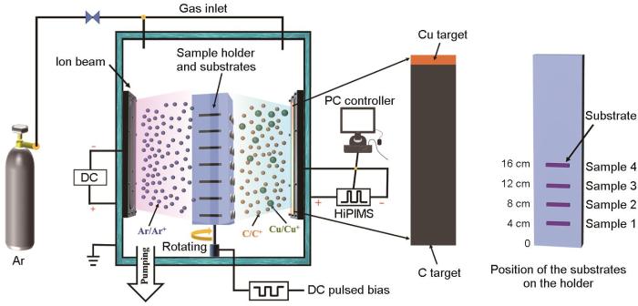
用高功率脉冲磁控溅射制备不同Cu掺杂含量非晶碳薄膜,其设备(图1)包括一个离子束源和一个磁控溅射源。磁控溅射用的靶材为Cu(99.99%, 20 mm × 100 mm)与石墨(99.99%, 380 mm × 100 mm)拼接靶,使用HiPIMS电源,工作气体为Ar气。衬底为二氧化硅、石英玻璃以及单面抛光单晶硅片。将用无水乙醇清洗干净的衬底固定在四面体机架,然后置于真空沉积腔室中。如图1所示,将距离机架底部4、8、12、16 cm的样品分别命名为S1、S2、S3、S4。待腔室真空度达到2.7×10⁻³ Pa后向腔室通入40 mL/min的Ar气,离子束工作电压设定为1200 V,对衬底进行刻蚀清洗20 min。调节Ar气流量使腔室的气压达1.3×10⁻² Pa。用HiPIMS电源沉积Cu掺杂非晶碳薄膜,溅射功率为500 W,频率为455 Hz,脉宽为200 μs。在机架上施加-200 V的偏压,并使其以120 Hz的频率自传。为了调控Cu含量,调整样品在机架上的位置以改变Cu靶与样品的靶基距。由于Cu的溅射产额大于C,因此越靠近Cu靶位置薄膜样品沉积速率越高。为了排除薄膜厚度对样品性能的影响,S1、S2、S3号样品的沉积时间为120 min,S4号样品的沉积时间为95 min,以使所有薄膜的厚度为205±20 nm。
图1
1.2 结构和性能表征
用热场发射扫描电子显微镜(SEM, Verios G4 UC)观察薄膜截面的形貌并测量其厚度。使用原子力显微镜(AFM)轻敲模式表征薄膜表面的形貌和粗糙度。使用X射线光电子能谱仪(XPS, Axis Ultra DLD)表征a-C: Cu薄膜的元素含量和化学键。测试前用4 kV的Ar+蚀刻样品4 min以去除表面污染物。用高斯和洛伦兹函数对C 1s峰进行分峰拟合,并计算sp2-C/sp3-C比例。用拉曼光谱(LAbRAMHR Evolution, 532 nm)分析a-C: Cu薄膜中碳原子键合结构。用X射线衍射仪(XRD, D8 ADVANCE DAVINCI)表征薄膜的相结构。用透射电子显微镜(TEM, Tecnai F20)表征薄膜的微观结构,根据电子能量损失谱(EELS)分析碳键结构。用紫外光电子能谱(UPS, Axis Ultra DLD)测量薄膜价带谱和二次电子截止边谱,其光源为能量21.22 eV的He I共振线。使用综合物理性能测试系统(PPMS, PPMS-EverCool)测量a-C: Cu薄膜在150~350 K的I-V特性和电阻率。使用紫外可见近红外分光光度计(Lambda 950)测量石英衬底上的薄膜在200~1600 nm范围的透过率并计算其光学带隙,测试间隔为1 nm,扫描速度为280 nm/min。
2 结果和讨论
2.1 薄膜的组分和结构
调控沉积时间,使a-C: Cu薄膜的厚度在186~221 nm范围变化。S1、S2、S3、S4样品的沉积速率分别为1.55、1.73、1.84和2.23 nm/min。随着样品靠近Cu靶,薄膜的沉积速率逐渐提高。图2给出了硅片上a-C: Cu薄膜截面的形貌。在Cu的含量较低时,Cu的掺入对薄膜的结构没有明显的影响,所有的薄膜均具有良好的致密性。同时,薄膜与Si衬底界面处也没有出现裂纹或剥落,表明a-C: Cu薄膜与衬底界面的结合良好。
图2
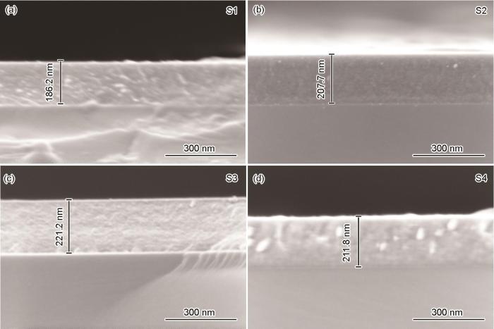
图2
Cu掺杂非晶碳薄膜截面的SEM形貌
Fig.2
SEM cross-sectional morphology of a-C:Cu films (a) S1, (b) S2, (c) S3, (d) S4
为了进一步研究Cu掺杂对非晶碳表面形貌的影响,用AFM表征了表面的形貌和粗糙度。图3给出了S1~S4样品的3D-AFM图像。可以看出,所有a-C: Cu薄膜的表面都连续和光滑,从S1到S4的粗糙度Ra分别为0.28、0.32、0.26、0.24 nm。Cu的掺入对非晶碳表面的粗糙度没有明显的影响,但是Cu含量不同的样品其表面形貌不同,S1、S2样品的表面凸起状结构较多,而S3、S4样品表面呈现更多的颗粒状结构。
图3
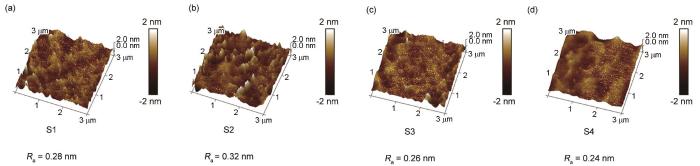
图3
Cu掺杂非晶碳薄膜的三维AFM表面形貌
Fig.3
3D-AFM images of a-C: Cu films (a) S1, (b) S2, (c) S3, (d) S4
图4给出了S1~S4样品的XPS光谱和拟合结果。图4a给出了全谱,可见所有a-C: Cu薄膜由C、Cu和O三种元素组成,其中O元素可能来自沉积过程中真空腔室中残余的空气[20,21]。如图4b所示,随着样品到机架底部的距离从4 cm逐渐增大到16 cm,Cu含量(原子分数)从2.77%提高到7.28%,表明实现了对Cu含量的调控。图4c给出了C 1s精细谱,为了得到sp2-C和sp3-C的相对含量,用高斯(80%)和洛伦兹(20%)函数将C 1s峰分为三个峰,分别对应结合能为284.6、285.4和286.6 eV的sp2-C、sp3-C和C-O/C=O[22]。如图4d所示,随着Cu含量的提高sp2-C的含量随之提高。Cu含量(原子分数,下同)为7.28%的sp2-C其含量最高(54%),原因可能是Cu元素的引入促进了sp2-C的形成[23, 24]。图4e给出了Cu 2p的精细谱,位于933和953 eV附近的峰对应Cu 2p3/2和Cu 2p1/2,在933.0和953.2 eV之间没有出现卫星峰,表明a-C: Cu薄膜中没有Cu2+[25, 26]。为了进一步判断薄膜中Cu的存在形式,测试了Cu的俄歇谱(图4f)。位于568.3 eV的峰表明,a-C: Cu薄膜中的Cu主要以单质的形式存在[27]。
图4

图4
Cu掺杂量不同的a-C: Cu薄膜的XPS全谱、各元素的含量、C 1s精细谱及各杂化碳含量、Cu 2p的精细谱以及Cu的俄歇谱
Fig.4
XPS spectra (a), the contents of C, O, Cu (b), C 1s spectra (c), sp2, sp3, and C-O/C=O contents (d), Cu 2p spectra (e) and Cu LMM Auger spectra (f) of a-C: Cu films with different Cu contents
图5a给出了不同Cu含量a-C: Cu薄膜的拉曼光谱。在波数为800~2000 cm-1样品S1~S4的谱中都出现了典型的非晶碳非对称拉曼峰。用高斯拟合将非晶碳拉曼峰分为位于1360 cm-1附近的D峰和1550 cm-1的G峰[28],其中D峰对应环状结构中sp2-C原子呼吸振动,G峰则对应环和链状结构中sp2-C原子的伸缩振动。根据G峰的半高宽(G-FWHM)、D峰与G峰的面积比(ID/IG)以及G峰位置(G-peak position),可定性分析sp2-C团簇的尺寸和含量。如图5b所示,随着Cu含量从2.7%提高到7.28%,ID/IG从2.2增大到2.6,表明Cu的掺入有利于增大sp2-C团簇的尺寸。G峰位也随着掺入Cu含量提高而增大,Cu含量为7.28%时G峰位置达到最大值1549.5 cm-1。G-FWHM先增大后减小,表明Cu含量的提高使a-C: Cu薄膜结构的无序度先提高后降低。
图5
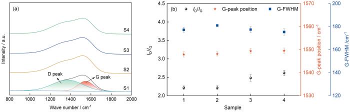
图5
Cu掺杂量不同的a-C: Cu薄膜的拉曼光谱及其拟合结果
Fig.5
Raman spectra (a), the fitting result (b) of a-C: Cu films with different Cu contents
图6给出了无衍射硅衬底上随Cu含量变化的a-C: Cu薄膜的XRD谱。可以看出,在所有样品的谱中均未出现明显的衍射峰,表明Cu含量为2.77%~7.28%的薄膜其主体仍为非晶态。
图6
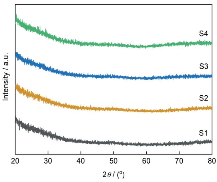
图6
Cu掺杂量不同的a-C:Cu薄膜的XRD谱
Fig.6
XRD spectra of a-C:Cu films with different Cu contents
为了进一步探究薄膜的微观结构和掺杂Cu的存在形式,对Cu含量为2.77%和7.28%的样品进行了TEM表征。如图7a所示,Cu含量为2.77%的薄膜均匀致密,在HRTEM图中未出现明显的晶格条纹,表明非晶碳中的Cu以固溶的形式存在。值得指出的是,在图7b对应SAED的图中,衍射环(R=4.43 nm-1)对应的是Pt(111)晶面(d=0.229 nm)。在Cu含量为7.28%的非晶碳基质中出现了尺寸约为5 nm的纳米晶(图7c),其SAED衍射环(R=4.76 nm-1)对应Cu的(111)晶面(d=0.209 nm)。这表明,随着Cu含量从2.77%提高到7.28%固溶在非晶碳中的Cu原子逐渐析出形成纳米晶,并均匀地分散镶嵌在非晶碳基质中。
图7
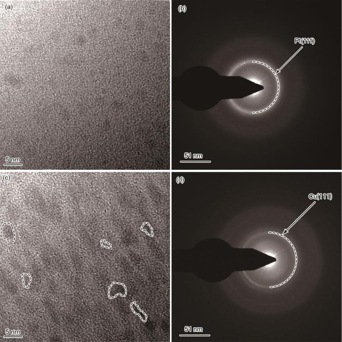
图7
Cu含量为2.77%和7.28%样品的高分辨电子图像和选区电子衍射图
Fig.7
HRTEM image and corresponding SAED of a-C: Cu film with 2.77% (a, b) and 7.28% Cu (c, d)
图8
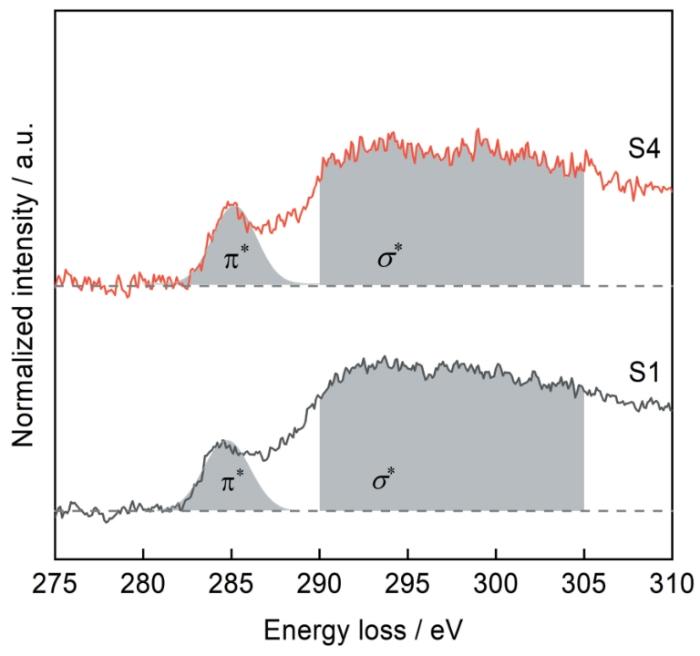
图8
Cu掺杂量为2.77%和7.28%样品的电子能量损失谱
Fig.8
EELS spectrum of a-C: Cu film with 2.77% and 7.28% Cu
2.2 电学性能
图9

图9
Cu掺杂量不同的a-C: Cu薄膜300 K时的 I-V特性曲线和电阻率的变化
Fig.9
I-V characteristic plots (a) and electrical resistiv-ity (b) at 300 K of the a-C: Cu films with differ-ent Cu contents
图10给出了S1~S4样品150~350 K的I-V曲线。在整体上,所有样品在各温度下都表现出优异的线性I-V特性。测试电流一定时每个样品对应的电压都随着测试温度的升高而降低,表明a-C: Cu薄膜均具有典型半导体特性。同时,在相同温度下,测试电流一定时Cu掺杂量小的样品对应的电压值高。例如S1样品对应的电压值在所有样品中最大,与S1样品的薄膜电阻率R更大有关。
图10
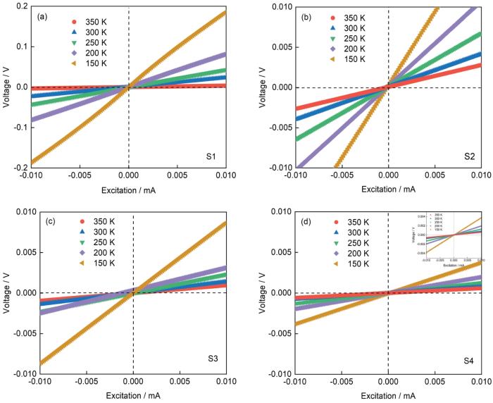
图10
Cu掺杂量不同的a-C: Cu薄膜在150~350 K的I-V曲线
Fig.10
I-V plots of the a-C: Cu films with different Cu contents from 150 to 350 K
图11

图11
Cu掺杂量不同的a-C: Cu薄膜在150~350 K的R-T曲线
Fig.11
R-T behaviors of a-C: Cu films with different Cu contents from 150 to 350 K
其中R为电阻率,T为测试温度,R0和T0皆为常数,n取值1、1/4和1/2,其载流子输运行为分别对应热激活,Mott型三维变程跳跃传导以及计入Coulomb作用的变程跳跃传导。
图12给出了S1~S4样品150~350 K的拟合结果。对于掺入Cu含量较高的S3(5.4% Cu,原子分数)和S4(7.28% Cu,原子分数)样品,在150~350 K其ln(R)与T-1/4线性关系较为显著,对应的载流子传输方式为Mott型三维变程跳跃传导,如图12e、f所示。而Cu掺杂含量较低的S1(2.77% Cu,原子分数)和S2(3.88% Cu,原子分数)样品,在整个测试温度区间没有显示出单一的传输机制,在不同温度范围载流子的输运特性不同。如图12a、c所示,在150~250 K样品S1、S2的ln(R)与T-1/4呈现线性关系;而在250~350 K,ln(R)与T-1则显示出线性关系,如图12b、d所示。因此,Cu含量为2.77%和3.88%样品在250~350 K其热激活主要为输运机制;而在150~250 K,起主要作用的是Mott型三维变程跳跃传导。
图12

图12
Cu掺杂量不同的a-C: Cu薄膜在不同温度范围的ln(R)与T-1/4和T-1的关系曲线
Fig.12
Relationship between ln(R) and T-1/4 (a, c, e, f) and T-1 (b, d) at different temperature ranges for the samples with different Cu contents. The red lines are fitting results
2.3 能带结构
图13
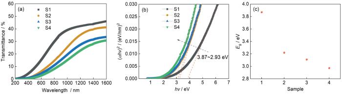
图13
Cu掺杂量不同的a-C: Cu薄膜的透过率曲线、(αhν)2-hν曲线以及光学带隙
Fig.13
Transmittance (a), Tauc plots (b) and optical bandgap (c) of a-C: Cu films with different Cu contents
计算其光学带隙。其中α为光吸收系数,hν为入射光子能量,A为常数,Eg为材料光学带隙,指数n(可取1/2、3/2、2和3)的值与半导体材料以及跃迁类型相关。绘制(αhν)1/n 与hν曲线并将其线性部分延长至α=0,则对应的入射光子能量即为光学带隙。光吸收系数α可用朗伯比尔定律[33]
计算,其中d为薄膜厚度,单位为nm;T为透过率。
电学测试结果表明,掺入原子分数为2.77%至7.28% Cu的a-C: Cu薄膜仍具有典型的半导体特性,因此可将其作为半导体处理。Pandey和Majeed指出,a-C为直接带隙半导体[10,32],n取1/2。图13b中S1~S4样品的(αhν)2-hν曲线,给出了Cu含量对a-C: Cu薄膜光学带隙的影响。如图13c所示,随着Cu含量的提高样品S1-S4的光学带隙从3.87 eV下降到2.93 eV,可能是sp2-C/sp3-C比例与结构的变化所致[34,35]。sp3-C只有σ键,sp2-C既有σ键又有π键。而与σ态相比,π电子更接近费米能级,其带隙主要由π电子控制[36]。非晶碳薄膜的光学带隙,可用于间接评估sp2-C的含量和团簇尺寸。其原因是,Eg随着sp2-C的含量的提高和团簇尺寸的增大而降低[23]。
根据能带理论,电子的传输与样品的功函数密切相关,用UPS可测得S1~S4样品的功函数。Ecut为样品二次电子截止边的切线与x坐标轴交点,如图14a所示,S1~S4样品的Ecut约为16.61 eV。其对应的功函数WF可从He I(21.22 eV)中减去Ecut得到[37],约为4.61 eV。Cu的掺入,对a-C: Cu薄膜的功函数没有明显的影响。图14b给出了S1~S4样品价带顶(Ev)相对于费米能级(EF)的位置。可以看出,随着Cu含量的提高Ev相对EF的距离逐渐从1.62 eV降低到1.33 eV。以真空能级0 eV为参考,结合用紫外可见近红外透过测试测得的光学带隙,S1~S4的能带结构如图14c所示。对于本征半导体,其费米能级位于禁带中间。但是随着掺入Cu含量从2.77%提高到7.28%,S1~S4样品的费米能级向价带偏移了0.29 eV。
图14
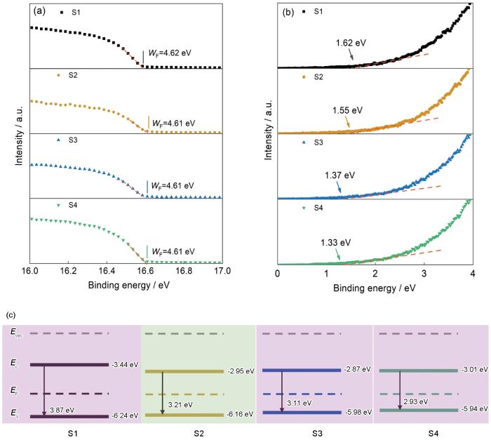
图14
不同Cu掺杂量a-C: Cu薄膜 的二次电子截至边、价带相对费米能级的位置以及 (c) 能带结构
Fig.14
Secondary electron cutoff (a), the distance from valence band (Ev) to the Fermi level (EF) (b) and band structure (c) of a-C: Cu films with different contents
3 结论
(1) 用HiPIMS溅射Cu-C拼接靶,可制备Cu含量为2.77%~7.28%的a-C: Cu薄膜。掺杂的Cu以单质态存在于非晶碳结构中。随着Cu含量从2.77%提高到7.28%固溶Cu原子析出生成纳米晶,sp2-C含量和团簇尺寸增大。
(2) 随着非晶碳中Cu掺杂量的提高a-C: Cu薄膜的导电性增强,薄膜的电学性能仍为典型的半导体特性,在150~350 K薄膜的电阻率均随着温度的升高而降低。Cu含量为5.4%和7.28%的样品在150~350 K其载流子的传导方式均为Mott型三维变程跳跃传导,而Cu含量为2.77%和3.88%的样品在250~350 K为热激活,在150~250 K则为Mott型三维变程跳跃传导。
(3) 随着薄膜中Cu掺杂量的提高a-C: Cu薄膜的光学带隙减小,费米能级则向价带偏移。
参考文献
High-temperature tribological behavior of Ti containing diamond-like carbon coatings with emphasis on running-in coefficient of friction
[J].
Effective target arrangement for detecting the properties of Ni doped diamond-like carbon by pulsed laser deposition
[J].
Triboelectrochemical friction control of W- and Ag-doped DLC coatings in water-glycol with ionic liquids as lubricant additives
[J].
In the last years, diamond like carbon (DLC) coatings doped with both carbide forming and non-carbide forming metallic elements have attracted great interest as novel self-lubricating coatings. Due to the inherent properties of DLC, the doping process can provide adsorption sites for lubricant additives depending on the chemical and electrochemical state of the surface. Ionic liquids (ILs) are potential lubricant additives with good thermal stability, non-flammability, high polarity, and negligible volatility. These characteristics make them also ideal for polar fluids, like water-based lubricants. In this work, three different DLC coatings (DLC, W- and Ag-doped DLC) were deposited on stainless steel substrates and their friction in dry and lubricated conditions in water-based lubricants was studied. Three ILs, tributylmethylphosphonium dimethylphosphate (PP), 1,3-dimethylimidazolium dimethylphosphate (IM) and 1-butyl-1-methylpyrrolidinium tris(pentafluoroethyl)trifluorophosphate (BMP) were used as additives and compared with a well-known organic friction modifier (dodecanoic acid). The results showed better mechanical integrity, toughness and adhesion of the doped coatings compared to the undoped DLC. The Ag-doped DLC coating had the best mechanical properties of all the coatings. W formed tungsten carbide precipitates in the DLC coating. Two different additive-adsorption mechanisms controlled friction: a triboelectrochemical activation mechanism for Ag-DLC, and an electron-transfer mechanism for W-DLC resulting in the largest reduction in friction.This journal is © The Royal Society of Chemistry.
Effects of deposition gas pressure on the properties of hydrogenated amorphous carbon nitride films grown by surface wave microwave plasma chemical vapor deposition
[J].
Amorphous carbon films for electronic applications
[J].
Thermal stable and low current complementary resistive switch with limited Cu source in amorphous carbon
[J].In this Letter, we report a complementary resistive switch (CRS) with good thermal stability and low ON current. The device is constructed with a bilayer structure composed of sputtered amorphous carbon (a-C) and thermal annealed Cu doped a-C (a-C:Cu). The Cu atoms in a-C:Cu can agglomerate to form nanosized active electrodes by thermal annealing. The Cu species can migrate and redistribute to form conductive filaments within the a-C and a-C:Cu layer through an electrochemical redox reaction. The depletion of Cu species in the a-C:Cu or a-C layer produces complementary resistive switching behaviors. Benefiting from the high thermal stability of a-C and a-C:Cu, the device works stable at a high temperature of up to 300 °C with an endurance of 104 switching cycle and narrow cycle-to-cycle distribution of threshold voltages. Furthermore, the effects of the Cu content in the a-C:Cu layer and the thickness ratio of a-C:Cu/a-C on the ON state current were studied. By limiting the content of Cu in the a-C:Cu layer, a low ON state current of 5 μA was obtained, which is among the lowest in the reported CRSs. Furthermore, a “stateful” material implication logic with the “0” and “1” states represented by a distinct combination of the resistance of each layer was implemented. The CRS is a potential and promising device for low power memory/computing applications and harsh electronics.
Diamond like carbon nanocomposites with embedded metallic nanoparticles
[J].
Effect of metal doping on structural characteristics of amorphous carbon system: a first-principles study
[J].
Effect of oxidation of copper nanoparticles on absorption spectra of DLC: Cu nanocomposites
[J].
Nickel concentration dependent structural and optical properties of electrodeposited diamond like carbon thin films
[J].
Giant negative piezoresistive effect in diamond-like carbon and diamond-like carbon-based nickel nanocomposite films deposited by reactive magnetron sputtering of Ni target
[J].
Absence of diffusion in certain random lattices
[J].
Electrical conduction properties of hydrogenated amorphous carbon films with different structures
[J].Hydrogenated amorphous carbon (a-C:H) films have optical and electrical properties that vary widely depending on deposition conditions; however, the electrical conduction mechanism, which is dependent on the film structure, has not yet been fully revealed. To understand the relationship between the film structure and electrical conduction mechanism, three types of a-C:H films were prepared and their film structures and electrical properties were evaluated. The sp2/(sp2 + sp3) ratios were measured by a near-edge X-ray absorption fine structure technique. From the conductivity–temperature relationship, variable-range hopping (VRH) conduction was shown to be the dominant conduction mechanism at low temperatures, and the electrical conduction mechanism changed at a transition temperature from VRH conduction to thermally activated band conduction. On the basis of structural analyses, a model of the microstructure of a-C:H that consists of sp2 and sp3-bonded carbon clusters, hydrogen atoms and dangling bonds was built. Furthermore, it is explained how several electrical conduction parameters are affected by the carrier transportation path among the clusters.
Study of variable range hopping conduction mechanism in nanocrystalline carbon thin films deposited by modified anodic jet carbon arc technique: application to light-dependent resistors
[J].
Electrical percolation threshold in Ag-DLC nanocomposite films prepared by RF-sputtering and RF-PECVD in acetylene plasma
[J].
Electro- and magneto-transport properties of amorphous carbon films doped with iron
[J].
Chemical bond structure of metal-incorporated carbon system
[J].
First principles investigation of interaction between impurity atom (Si, Ge, Sn) and carbon atom in diamond-like carbon system
[J].
Stress reduction mechanism of diamond-like carbon films incorporated with different Cu contents
[J].
Electrochemical pulsed deposition of diamond-like films by powerful coulostatic discharge in dimethylsulfoxide solution of lithium acetylide
[J].
Formation of rod-shaped wear debris and the graphitization tendency of Cu-doped hydrogenated diamond-like carbon films
[J].
Structure and optical properties of Cu-DLC composite films deposited by cathode arc with double-excitation source
[J].
Microstructure and mechanical properties of Mo/DLC nanocomposite films
[J].
Highly efficient and robust Cu catalyst for non-oxidative dehydrogenation of ethanol to acetaldehyde and hydrogen
[J].
Accommodation of silicon in an interconnected copper network for robust Li-ion storage
[J].
Quasi-graphitic carbon shell-induced Cu confinement promotes electrocatalytic CO2 reduction toward C2+ products
[J].For steady electroconversion to value-added chemical products with high efficiency, electrocatalyst reconstruction during electrochemical reactions is a critical issue in catalyst design strategies. Here, we report a reconstruction-immunized catalyst system in which Cu nanoparticles are protected by a quasi-graphitic C shell. This C shell epitaxially grew on Cu with quasi-graphitic bonding via a gas–solid reaction governed by the CO (g) - CO2 (g) - C (s) equilibrium. The quasi-graphitic C shell-coated Cu was stable during the CO2 reduction reaction and provided a platform for rational material design. C2+ product selectivity could be additionally improved by doping p-block elements. These elements modulated the electronic structure of the Cu surface and its binding properties, which can affect the intermediate binding and CO dimerization barrier. B-modified Cu attained a 68.1% Faradaic efficiency for C2H4 at −0.55 V (vs RHE) and a C2H4 cathodic power conversion efficiency of 44.0%. In the case of N-modified Cu, an improved C2+ selectivity of 82.3% at a partial current density of 329.2 mA/cm2 was acquired. Quasi-graphitic C shells, which enable surface stabilization and inner element doping, can realize stable CO2-to-C2H4 conversion over 180 h and allow practical application of electrocatalysts for renewable energy conversion.
Interpretation of Raman spectra of disordered and amorphous carbon
[J].
The effect of Argon ion irradiation on the thickness and structure of ultrathin amorphous carbon films
[J].
Sputter deposition of dense diamond-like carbon-films at low-temperature
[J].Thin carbon films were deposited by ion beam sputtering at temperatures of 77–1073 K. Using Rutherford backscattering spectrometry and electron energy loss spectroscopy, the trends in film density and bonding were examined as a function of deposition conditions. It has been found that film density and sp3 bonding character unexpectedly increased with increased substrate thermal conductivity and decreasing substrate temperature, reaching values of 2.9 g/cc and 50%, respectively.
The multilayered structure of ultrathin amorphous carbon films synthesized by filtered cathodic vacuum arc deposition
[J].
Structural and optical properties of gold-incorporated diamond-like carbon thin films deposited by RF magnetron sputtering
[J].
Effect of nickel incorporation on the optical properties of diamond-like carbon (DLC) matrix
[J].
Optical and microstructural properties of diamond-like carbon films grown by pulsed laser deposition
[J].
Recombination and photoluminescence mechanism in hydrogenated amorphous carbon
[J].
Pulsed laser deposition and characterization of multilayer metal-carbon thin films
[J].
Interfacial engineering of Bi2S3/Ti3C2T x MXene based on work function for rapid photo-excited bacteria-killing
[J].In view of increasing drug resistance, ecofriendly photoelectrical materials are promising alternatives to antibiotics. Here we design an interfacial Schottky junction of Bi2S3/Ti3C2Tx resulting from the contact potential difference between Ti3C2Tx and Bi2S3. The different work functions induce the formation of a local electrophilic/nucleophilic region. The self-driven charge transfer across the interface increases the local electron density on Ti3C2Tx. The formed Schottky barrier inhibits the backflow of electrons and boosts the charge transfer and separation. The photocatalytic activity of Bi2S3/Ti3C2Tx intensively improved the amount of reactive oxygen species under 808 nm near-infrared radiation. They kill 99.86% of Staphylococcus aureus and 99.92% of Escherichia coli with the assistance of hyperthermia within 10 min. We propose the theory of interfacial engineering based on work function and accordingly design the ecofriendly photoresponsive Schottky junction using two kinds of components with different work functions to effectively eradicate bacterial infection.
