


第三代半导体碳化硅器件优异的物理、化学和力学性能,如电子能带结构[1]、优异的光学性能[2]、优异的热导率[3]、较高的化学惰性和优异的耐腐蚀性[4],使其在微/纳机电系统,核燃料组件、微电子元件和光电子器件等方面有广阔的应用前景。第三代半导体碳化硅器件,也是微电子整流器、微型探测器与传感器以及微型集成电路等国家重大亟需领域的核心器件。但是,微/纳机电系统的微型半导体电子元器件在复杂工况耦合因素影响下和频繁往复接触运动中,表面产生的黏着磨损使其耐久性服役寿命短、残次品率高和接触力学性能下降[5]。微/纳机电系统的微齿轮传动啮合部和轴承滚珠与滚道循环摩擦接触部位,以及硬盘存储器的磁头与磁盘往复滑动接触部位,在微观表/界面力、高速重载、极端使役温度耦合诱导下两器件表面产生黏着磨损,使半导体器件因脆性断裂产生磨粒而粘附于器件表面,导致微机电系统元器件接触失效和产生巨大的摩擦能耗[6]。了解在极端使役温度半导体器件接触时的动态变形特性和定量评估其接触力学性能和知悉元器件的损伤机制,有利于延长半导体器件的服役寿命。因此,深入研究半导体碳化硅器件的亚表层损伤行为、接触力学性能、相变转化规律并揭示其亚表层微观塑性特性与破坏机制显得极为必要。
目前对半导体器件接触的研究主要集中于分子动力学模拟(MD),主要研究其接触的微观力学变形行为与损伤机制。Zhang等[7]用MD法研究了单晶硅纳米压痕变形机制,发现受载下的单晶硅原子发生立方结构向体心结构的相变结构转化,并在压痕接触周围产生大量的非晶结构原子。Zhao等[8]用MD法研究了温度对单晶硅力学性能的影响,发现随着温度的降低单晶硅的弹性模量增大。Chen等[9]用MD法研究了温度对单晶硅纳米压痕接触变形的影响,发现受载下的单晶硅发生相变结构转化,使受载区域的接触原子粘附于探针的外表面,并随温度的升高粘着原子数量逐渐增多。施渊吉等[10]用MD法研究了多晶碳化硅纳米压痕的变形行为。结果表明,随着温度的升高多晶碳化硅的承载性能逐渐下降,位错从晶界形核处逐渐长大并向晶体内部扩张,最终形成位错环结构。另有相关学者研究了碳化硅位错滑移和无定形发生控制的相关塑性变形行为[11~14]。Zhao等[15]从微观角度揭示了β-SiC材料在室温下的塑性变形行为和脆性断裂特征。结果表明,表面裂纹的形貌对宏观力学性能有显著的影响。Kondo等[16]研究了不同辐照环境下β-SiC材料的蠕变变形。Zhao等[17]观察到,在极高压条件下碳化硅接触区域的非晶态原子层局部集中生成纳米带。Branicia等[18]用MD模拟研究了单位错核在冲击载荷作用下主导立方晶碳化硅的塑性变形机制。Chavoshi等[19]用原子水平方法研究了β-SiC材料高温纳米切削过程,发现位错形核和层错的形成是影响塑性初始变形的主要因素。鉴于此,本文构建第三代半导体典型碳化硅器件与虚拟压头接触的原子尺度物理模型,基于纳米压痕法研究半导体碳化硅器件接触时的亚表层损伤行为与破坏机制,并分析极端使役温度对受载诱导产生的位错环演变特征、相变转化数额、接触力学性能、亚表层损伤行为的影响。
1 基于分子动力学理论的计算
1.1 MD的设置
图1给出了(111)面单晶碳化硅的原子尺度物理模型,其长宽高分别为LX =16 nm、LY =21.5 nm和LZ =11.3 nm。建模时球形刚性金刚石压头的半径R=4 nm。球形刚性金刚石压头是施加载荷对象。碳化硅的晶格常数为0.45382 nm,金刚石的晶格常数为0.3567 nm。为了避免纳米尺度表界面效应和尺寸效应的影响,模拟时设置碳化硅的边界条件,碳化硅物理模型的XY轴采用周期性边界条件,Z轴采用非周期性边界条件。为了防止基底原子热运动中原子位置的迁移降低计算精度[20],固定碳化硅最底层为5层原子,限制其力与位移为零。此外,为了确保模拟结果的准确性和可靠性,将碳化硅基底划分为三层,即固定层原子、恒温层原子和牛顿层原子。固定层的厚度为2 nm,恒温层的厚度为2 nm,牛顿层的厚度为7.3 nm。用朗之万控温法控制恒温层原子的温度为300 K,恒温层原子与牛顿层原子,统称为运动层原子。赋予运动层原子的初始温度为300 K。基于NVE系综和Verlet算法积分求解运动层原子的牛顿方程,模拟时间步长为1fs[21~23]。体系弛豫30 Ps后,达到热力学平衡态。使用开源LAMMPS软件和Ovito完成整个计算[24]。模拟接触时,金刚石压头以40 m/s的恒定速度沿Z轴(
图1
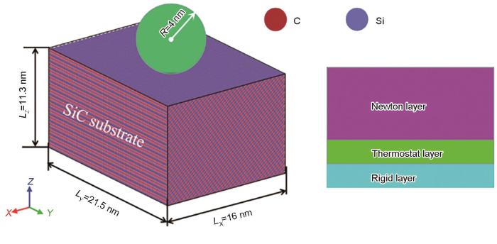
图1
纳米压痕接触中单晶碳化硅原子尺度物理模型与MD模拟示意图
Fig.1
Atomic scale physical model and MD simulation of single crystal silicon carbide during nanoindentation contact
1.2 势函数和位错的识别
为了准确描述碳化硅内部结构受到接触载荷产生的亚表层损伤,使用能有效描述碳化硅相变类型的vashishta势函数。可使用公式
计算总能量。其中的
1.3 应力和接触力学性能
材料受到的应力超过失效临界值时发生亚表层损伤,与内应力集中的von Mises stress有十分密切联系。因此,用von Mises stress定性表征材料亚表层损伤的内应力集中度[24],即
其中σxx 、σyy 、σzz 、τxy 、τyz 、τzx 分别为应力张量分量。且用剪切应变描述接触区域的碳化硅亚表层损伤行为,其中ηxx 、ηyy 、ηzz 、ηxz 、ηxy 、ηyz 为剪切应变分量。
Oliver-Pharr等[31]基于载荷与压深曲线,推导出P与H间关系
其中,
2 结果和讨论
2.1 单晶碳化硅基底亚表层的损伤行为
图2
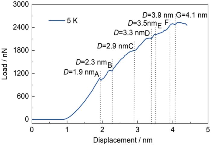
图2
低温(5K)下单晶碳化硅接触中的载荷与位移曲线关系
Fig.2
Relation of load and displacement curve in contact of single crystal silicon carbide at low temperature (5 K)
图3给出了采用DXA法[22]识别低温5K加载接触时碳化硅内部微结构的演化情形。图3表明,在下降位移D=1.9 nm时碳化硅内部位错形核成位错环,表明基底内部发生了塑性变形,亚表层发生了以位错成环形式的损伤。在下降位移D=1.9 nm至D=2.1 nm时,位错环产生滑移并扩张并出现增长和增大的趋势。在位移下降到D=2.3 nm时部分位错环开始增殖繁衍(图3箭头指示),另一部分位错环间发生交互作用形成了新的位错环。当载荷持续增加即位移下降到D=2.5 nm时位错环继续繁衍增殖,原有的位错环溟灭,新位错因位错环间的交互作用而产生。此外,位错环的扩张表明,碳化硅基底内亚表层发生了严重的损伤及扩展程度。从下降位移D=1.9 nm到D=2.5 nm,整个位错环历经三个阶段,即位错环形核、位错环生长增大和位错环繁衍增殖。下降位移D=2.7 nm到D=3.3 nm时部分位错环继续滑移增大和繁衍增殖并产生螺杆位错、刃位错和螺旋位错,详细演化过程在图4a、b中给出。由于位错环间的交互作用部分位错依然出现溟灭,新位错在载荷的诱导下产生。随着载荷的进一步增大,螺杆位错断裂形成棱柱型位错环并向基底底部发射。
图3
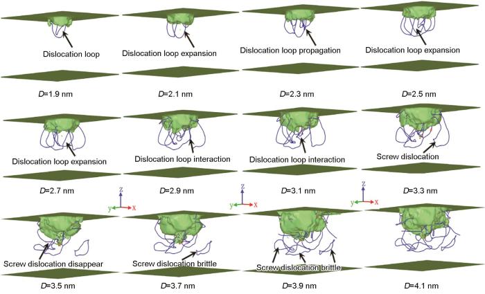
图3
低温(5K)下单晶碳化硅纳米压痕接触中亚表层损伤的微结构演化特征
Fig.3
Microstructure evolution of single crystal SiC during nanoindentation contact at low temperature (5 K)
图4
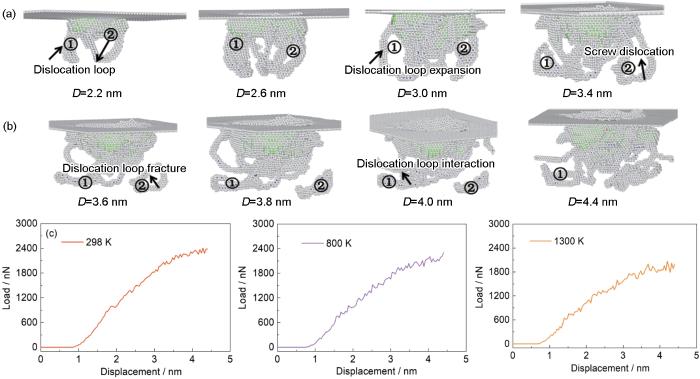
图4
低温(5 K)下单晶碳化硅螺杆位错脆断的演化进程与温度对碳化硅的载荷与位移曲线的影响
Fig.4
Evolution of brittle fracture of single crystal silicon carbide screw dislocation at low temperature (5 K) and influence of temperature on load and displacement curves of silicon carbide
图4a、b给出了位错环①与位错环②的脆断演化进程。可以看出,开始接触时碳化硅基底接触的正下方堆积很多位错源,在接触初期D=2.2 nm时在堆积的位错源的边缘两侧出现位错环①与位错环②形核,随后在载荷的作用下位错环①与位错环②开始生长增大并繁衍出新的位错环。到加载位移D=3.4 nm时位错环①演变为螺旋位错,位错环②逐渐演变为螺杆位错。随着加载位移的持续增大螺杆位错②发生脆断而形成棱柱形位错环,螺旋位错①也发生脆断。加载位移从D=3.8 nm增大到D=4.0 nm时,螺旋位错①与附近繁衍的新位错发生交互作用而形成新的螺旋位错,螺杆位错②与附件位错环没有交互作用产生依然保持位错环的脆断模式向基底底部发射运动。图4c给出了温度对碳化硅基底载荷与位移曲线的影响。可以看出,极端低温和高温对碳化硅的载荷与位移曲线有显著的影响。温度越高则碳化硅的载荷与位移曲线波动幅度越大,碳化硅的最大承载性逐渐降低,在接触的初期(弹性变形阶段)载荷与位移曲线波动式增加。其主要原因是,温度越高碳化硅基底被软化的程度越高。
图5给出了单晶碳化硅受纳米压痕接触载荷后表面形貌的变化,以及极端使役温度的影响。从图5a可见,在低温(5 K)下碳化硅亚表层的损伤最严重,在高温(1300 K)下碳化硅亚表层的损伤最轻。这表明,随着极端使役温度的升高单晶碳化硅基底亚表层损伤减轻,而表面的滑移程度加剧。同时,碳化硅表面生成了很多随机粗糙斑点,容易使黏着接触失效。从图5b可见,在高温下碳化硅的剪切变形程度剧烈,在低温5 K下碳化硅的表面极易产生剪切滑移带;在高温(800 K)下剪切滑移带易重构成位错环构型(图5b箭头指示)并随着极端高温的上升而演化。此外,在高温下碳化硅表面的随机粗糙斑点越加突出,与图5a给出的表面形貌受使役温度差异的影响一致。从图5c可见,碳化硅属于脆性材料,极端使役温度对碳化硅与压头间紧密接触边缘产生的磨粒有重要的影响。温度越高则紧密接触边缘产生的磨粒数越多,剪切滑移带边缘处的磨粒数也多。同时,表面接触边缘的磨粒数越多,则半导体碳化硅器件接触时更易发生黏着接触失效,磨粒在两接触体界面间形成第三体并刻化基底亚表面,从而加剧基体碳化硅表面的损伤行为。
图5
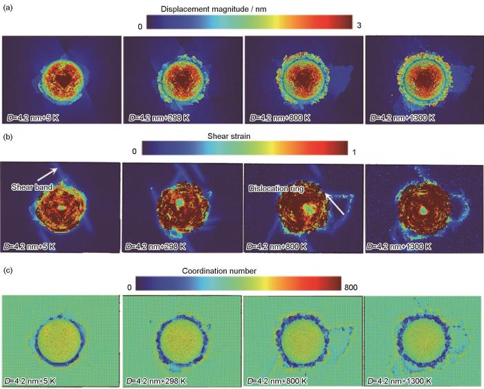
图5
极端使役温度对单晶碳化硅纳米压痕接触中表面形貌的影响
Fig.5
Effect of extreme active temperature on surface morphology of single crystal silicon carbide during nanoindentation contact
2.2 单晶碳化硅基底亚表层损伤力学性能和相变
为了更好地描述单晶碳化硅纳米压痕时的接触性能,定量评估了受载产生的力学性能随温度的变化。从图6a、b可见,使役温度为5 K、298 K、800 K以及1300 K时碳化硅基底的最大承载性分别为2496.26、2380.23、2212.36、1985.54,硬度分别为51.78、49.38、45.89、41.19,杨氏模量分别为116.86、111.43、103.57、92.95,接触刚度分别为911.04、868.69、807.43、724.64。从极端低温5 K到极端高温1300 K,最大承载性、硬度、杨氏模量、接触刚度都下降20.4%。此外,随着温度的升高最大承载性、硬度、杨氏模量、接触刚度曲线以类抛物线趋势下降。这表明,温度的升高使碳化硅亚表层材料的力学性能逐渐下降,更易发生静动载荷的损伤。从图6c可见,随着温度的升高碳化硅基底产生的位错密度呈线性增加趋势。温度越高则碳化硅基体晶格越容易膨胀,易产生更多的位错(6d),从而使材料的力学性能急剧降低。
图6
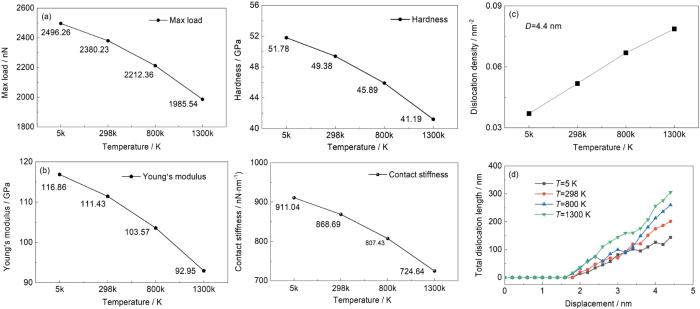
图6
单晶碳化硅纳米压痕时材料力学性能随使役温度的变化
Fig.6
Variation of mechanical properties of single crystal silicon carbide with service temperature during nanoindentation contact
图7

图7
单晶碳化硅基底亚表层损伤结构类型转化随温度的变化
Fig.7
The change of damage structure type of single crystal silicon carbide substrate with temperature
表1 单晶碳化硅亚表层损伤的相变结构类型转化数目随使役温度的变化
Table 1
| Loading | Temperature / K | |||||||||||
|---|---|---|---|---|---|---|---|---|---|---|---|---|
| Variable | 5 | 298 | 800 | 1300 | 5 | 298 | 800 | 1300 | 5 | 298 | 800 | 1300 |
| Depth / nm | Other structure | CD1st+CD2nd structure | HD+HD1st+HD2nd structure | |||||||||
| 0 | 0 | 0 | 0 | 0 | 0 | 0 | 0 | 0 | 0 | 0 | 0 | 0 |
| 2 | 528 | 885 | 1072 | 1203 | 18089 | 18367 | 18834 | 19795 | 0 | 0 | 192 | 464 |
| 2.4 | 2080 | 1627 | 1424 | 1336 | 19140 | 19598 | 20189 | 21094 | 0 | 57 | 611 | 1823 |
| 3 | 4096 | 2996 | 2793 | 2526 | 21856 | 21321 | 22381 | 23249 | 70 | 448 | 1118 | 3454 |
| 4 | 9223 | 6289 | 4990 | 4460 | 25263 | 26353 | 27356 | 28742 | 155 | 510 | 2674 | 6165 |
| 4.4 | 11792 | 7854 | 5539 | 5735 | 26886 | 28221 | 29124 | 30354 | 176 | 637 | 3550 | 7928 |
2.3 单晶碳化硅基底亚表层损伤和破坏的机制
图8给出了单晶碳化硅的von Mises stress随着极端低中高使役温度的变化,可以看出,使役温度对碳化硅应力有显著的影响。无论使役温度是低温还是高温,碳化硅基底的应力集中主要在亚表层,其次是表层应力。碳化硅内亚表层的微结构演化与滑移处的富集大量应力,使微结构发生迁移与演变和产生新的位错以及旧位错发生溟灭。应力集中,是导致碳化硅材料亚表层损伤和破坏的关键因素。使役温度为低温5 K时碳化硅基底紧密接触边缘两侧分布的应力较集中且呈现均匀化,随着使役温度的升高该区域的应力越加集中。同时,温度越高则材料软化的程度越高,碳化硅基底晶格受迫产生的剧烈程度越强,越易出现晶格点阵的破坏,从而使应力更易集中,材料的亚表层损伤随之严重,最终导致材料的力学性能急剧下降,接触性能大大降低。另外,无论是在低温还是高温,压痕中接触区两侧不断产生应力集中,两侧区的应力集中随压深而增加,使应力集中加剧且范围更广。其主要原因是,压头位移的持续增加使碳化硅基底受到更大的载荷冲击,导致接触边缘两侧位错环 的不断迁移演化而产生亚表层损伤。
图8
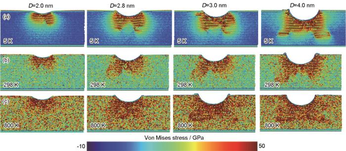
图8
单晶碳化硅纳米压痕受载诱导的von Mises stress随使役温度的变化
Fig.8
The change of load-induced von Mises stress of single crystal silicon carbide during nanoindentation with the operating temperature
3 结论
(1) 根据分子动力学,纳米压痕受载时碳化硅基底发生塑性变形,使其亚表层的损伤主要以位错形核堆积、位错滑移、位错成环形式发生塑性变形。在极端低温(5 K)下位错环的形成历经位错形核、位错环生长增大、位错环繁衍增殖和位错环脆断四个阶段。部分位错环溟灭而新位错则因位错环间的交互作用而产生。载荷诱导的持续作用使碳化硅基底内亚表层发生了严重程度的损伤和扩展。温度越高则碳化硅基底产生的位错总长越大。
(2) 极端使役温度对脆性碳化硅与压头间紧密接触边缘产生的磨粒数有重要的影响,温度越高则紧密接触边缘产生的磨粒数越多,且剪切滑移带边缘处的磨粒数越多。同时,表面接触边缘的磨粒数越多,则半导体碳化硅器件接触时更易产生黏着接触失效,使磨粒在两接触体界面间产生第三体作用。
(3) 碳化硅基底的内应力集中是材料亚表层发生损伤及相变和立方碳化硅向闪锌矿碳化硅类型转变的根本原因。应力集中集中在材料亚表层形核与滑移处。随着温度的升高碳化硅材料的最大承载性、硬度、杨氏模量以及接触刚度曲线呈现类抛物线趋势下降。温度越高则碳化硅基体晶格点阵越容易膨胀,更多位错的产生导致材料应力集中,使碳化硅材料的接触力学性能急剧降低。
参考文献
Elevated-temperature behavior of high-strength silicon carbide
[J].
Thermal expansion coeffificient of 3C-SiC
[J].
Theoretical results for the temperature dependence of the thermal expansion coefficient for 3C–SiC are reported using a phenomenological lattice dynamical theory in the quasiharmonic approximation. The linear thermal expansion coefficient α of 3C–SiC exhibits a variation with temperature much like that of the specific heat and, unlike other tetrahedrally coordinated materials, it does not attain a negative value at lower temperatures.
Dislocations in 4H-and 3C-SiC single crystals in the brittle regime
[J].
Quantum confinement effects on electronic properties of hydrogenated 3C-SiC nanowires
[J].
Concerning and developing tribology, promoting sustainable economic development
[J].
Mechanical Engineering Development Strategy Report (2011-2020)
[R] Beijing:
机械工程学科发展战略报告(2011-2020)
[R].
Evolution of metastable phases in silicon during nanoindentation: mechanism analysis and experimental verification
[J].
Molecular dynamics investigations of temperature effects on the nano-indentation/scratching response of typical single crystal materials
[D].
温度对典型单晶材料纳米压痕/划痕响应影响的分子动力学解析
[D].
Original analysis of adhesion produced for semiconductor silicon device based on atomic simulation
[J].
Deformation mechanism of nanoscale polycrystalline α-silicon carbide based on molecular dynamics simulation
[J].
基于分子动力学模拟的纳米多晶α-碳化硅变形机制
[J].在考虑晶界和温度效应影响的条件下,基于分子动力学法使用Vashishta势函数研究多晶α-碳化硅基体在纳米压痕作用下的塑性变形机制,分析载荷位移曲线并通过识别变形结构描述了变形区域中的原子破坏和迁移轨迹变化。在下压过程中,因接触载荷不断增大在接触区的晶粒内产生无定型化相变并不断向晶体内部扩展,扩展到晶界处被阻碍住。随着载荷的持续增大,晶界作为位错发射源在高应力水平下出现1/2〈110〉全位错滑移。同时,随着温度的升高α-碳化硅多晶的承载能力下降,特别是材料内部出现塑性变形,位错从晶界处形核长大并向晶体内部扩展,最后形成‘U型’位错环。
Interfacial plasticity controls material removal rate during adhesive sliding contact
[J].
Simultaneously increasing the strength and ductility of a refractory high-entropy alloy via grain refining
[J].
In-situ observation of the initiation of plasticity by nucleation of prismatic dislocation loops
[J].
A numerical study on the material removal and phase transformation in the nanometric cutting of silicon
[J].
Depth-sensing ductile and brittle deformation in 3C-SiC under Berkovich nanoindentation
[J],
Irradiation creep of 3C-SiC and microstructural understanding of the underlying mechanisms
[J].
Shock-induced amorphization in silicon carbide
[J].
Nanoductility induced brittle fracture in s high performance ceramics
[J].Nanoductility induced crack nucleation mechanism mediated by a single dislocation core is revealed in a 300 million-atom molecular dynamics simulation of shocked silicon carbide ceramic. The atomistic damage mechanism involves dynamic transitions between clearly delineated regimes—from shock-induced structural transformation to plastic deformation to brittle fracture. Such atomistic understanding may help in the design of nanocrack suppression strategies to realize predictive modeling of complex damage processes in high-performance ceramics.
Molecular dynamics simulation study of deformation mechanisms in 3C-SiC during nanometric cutting at elevated temperatures
[J].
Formation of prismatic loops in AlN and GaN under nanoindentation
[J].
Effect of adhesive contact failures on single crystal copper with different diamond radius
[J].
金刚石探针曲率半径对单晶铜表面粘附接触失效影响分析
[J].
Molecular dynamics simulation of failure in adhesive contact with single crystal copper
[J].
纳观单晶铜表面粘着接触失效的分子动力学模拟
[J].
Plastic deformation in zinc-blende AlN under nanoindentation: A molecular dynamics simulation
[J].
Visualization and analysis of atomistic simulation data with OVITO-the open visualization tool
[J].
Synergistic effects of twin boundary and phase boundary for enhancing ultimate strength and ductility of lamellar TiAl single crystals
[J].
A newly developed interatomic potential of Nb-Al-Ti ternary systems for high-temperature applications
[J].
Twinning anisotropy of tantalum during nanoindentation
[J].
An improved technique for determining hardness and elastic modulus using load and displacement sensing indentation experiments
[J].The indentation load-displacement behavior of six materials tested with a Berkovich indenter has been carefully documented to establish an improved method for determining hardness and elastic modulus from indentation load-displacement data. The materials included fused silica, soda–lime glass, and single crystals of aluminum, tungsten, quartz, and sapphire. It is shown that the load–displacement curves during unloading in these materials are not linear, even in the initial stages, thereby suggesting that the flat punch approximation used so often in the analysis of unloading data is not entirely adequate. An analysis technique is presented that accounts for the curvature in the unloading data and provides a physically justifiable procedure for determining the depth which should be used in conjunction with the indenter shape function to establish the contact area at peak load. The hardnesses and elastic moduli of the six materials are computed using the analysis procedure and compared with values determined by independent means to assess the accuracy of the method. The results show that with good technique, moduli can be measured to within 5%.
Nanoindentation of γ-TiAl with different Crystal planes by molecular dynamics simulations
[J].The periodicity and density of atomic arrangement vary with the crystal orientation, which results in different deformation mechanisms and mechanical properties of γ-TiAl. In this paper, the anisotropic characteristics for γ-TiAl with (100), ( 1 ¯ 10 ) and (111) surfaces during nanoindentation at 300 K have been investigated by molecular dynamics simulations. It is found that there is no obvious pop-in event in all load-depth curves when the initial plastic deformation of γ-TiAl samples occurs, because the dislocation nucleates before the first load-drop; while a peak appears in both the unloading curves of the ( 1 ¯ 10 ) and (111) samples due to the release of energy. Stacking faults, twin boundaries and vacancies are formed in all samples; however, interstitials are formed in the (100) sample, a stacking fault tetrahedron is formed in the (111) sample; and two prismatic dislocation loops with different activities are formed in the ( 1 ¯ 10 ) and (111) samples, respectively. It is also concluded that the values of the critical load, strain energy, hardness and elastic modulus for the (111) sample are the maximum, and for the (100) sample are the minimum. Furthermore, the orientation dependence of the elastic modulus is greater than the hardness and critical load.
Simulation of nanometer-scale deformation of metallic and ceramic surfaces
[J].
