Thermal management and packaging of wide and ultra-wide bandgap power devices: a review and perspective
1
2023
... 基于金属-半导体结的肖特基二极管(Schottky barrier diode, SBD)的正向压降较低、超高速响应和低功耗,得到了广泛的应用[1,2].SBD的整流特性和稳定性决定于其金属-半导体势垒,常用的势垒金属有Au[3]、Pt[4]、Ni[5]和Pd[6].但是,这些传统贵金属的热稳定性较低且功函数不可调.使用合金材料替代单一贵金属可精准调控势垒高度[7,8].镍铂(NiPt)合金的热稳定性较高且界面特性可调控,是主流势垒材料[9~11].制备NiPt基SBD用的是在Si基底磁控溅射的合金薄膜,将其热处理形成热稳定的NiPtSi势垒层可实现反向电流阻断[12].关于NiPt合金的研究,侧重于NiPt薄膜与Si形成的势垒高度[13]、热稳定性[11]以及高速退火工艺等方面[14].制备NiPt合金薄膜的工艺参数对SBD器件势垒层微结构和性能的影响尚须进一步深入研究[15~17].近年来,研究人员通过调控磁控溅射制备参数(如沉积时间、基底温度和沉积速率等)改善NiPt合金薄膜的表面粗糙度并调控残余应力[9,18,19].Shin等[18]用晶圆曲率法研究了xNi(1-x)Pt (0.02 < x < 0.81)薄膜的应力行为,发现富集Ni的样品对基底温度和沉积速率的变化极其敏感.随着基底温度的降低和沉积速率的提高,薄膜中的残余应力显著增大.Eiler等[19]分析了xNi(1-x)Pt (0.01 < x < 0.39)薄膜的杨氏模量和硬度的变化,发现随着沉积时间的延长表面粗糙度有所提高.Yang等[20]发现,基底取向对ZnO薄膜的表面粗糙度也有显著影响.取向不同的基底其原子排列不同,使在其上制备的薄膜原子的生长能力也不同.在Si(100)基底上制备的薄膜表面粗糙度略比Si(111)基底的低.Tsamouras和Galinski等[21,22]发现,随着基底温度的提高在其上制备的Pt薄膜表面粗糙度提高,因为基底原子的扩散增强和活化能增大.虽然有些工作研究了用不同工艺制备的NiPt合金薄膜的表面粗糙度和残余应力状态的变化,但是关于制备工艺参数不同的Ni5Pt合金薄膜的应力变化和薄膜表面质量仍缺少系统的研究[10,16,23],特别是亟需进一步揭示薄膜制备工艺参数对薄膜的残余应力和表面粗糙度的影响.鉴于此,本文在两种晶体取向的单晶硅基底上磁控溅射Ni5Pt合金薄膜,研究基底温度、沉积时间以及基底取向对薄膜的表面粗糙度和微观结构的影响,并根据薄膜的开裂行为以及残余应力分布建立薄膜开裂的判据. ...
Role of interfacial oxide in high-efficiency graphene-silicon Schottky barrier solar cells
1
2015
... 基于金属-半导体结的肖特基二极管(Schottky barrier diode, SBD)的正向压降较低、超高速响应和低功耗,得到了广泛的应用[1,2].SBD的整流特性和稳定性决定于其金属-半导体势垒,常用的势垒金属有Au[3]、Pt[4]、Ni[5]和Pd[6].但是,这些传统贵金属的热稳定性较低且功函数不可调.使用合金材料替代单一贵金属可精准调控势垒高度[7,8].镍铂(NiPt)合金的热稳定性较高且界面特性可调控,是主流势垒材料[9~11].制备NiPt基SBD用的是在Si基底磁控溅射的合金薄膜,将其热处理形成热稳定的NiPtSi势垒层可实现反向电流阻断[12].关于NiPt合金的研究,侧重于NiPt薄膜与Si形成的势垒高度[13]、热稳定性[11]以及高速退火工艺等方面[14].制备NiPt合金薄膜的工艺参数对SBD器件势垒层微结构和性能的影响尚须进一步深入研究[15~17].近年来,研究人员通过调控磁控溅射制备参数(如沉积时间、基底温度和沉积速率等)改善NiPt合金薄膜的表面粗糙度并调控残余应力[9,18,19].Shin等[18]用晶圆曲率法研究了xNi(1-x)Pt (0.02 < x < 0.81)薄膜的应力行为,发现富集Ni的样品对基底温度和沉积速率的变化极其敏感.随着基底温度的降低和沉积速率的提高,薄膜中的残余应力显著增大.Eiler等[19]分析了xNi(1-x)Pt (0.01 < x < 0.39)薄膜的杨氏模量和硬度的变化,发现随着沉积时间的延长表面粗糙度有所提高.Yang等[20]发现,基底取向对ZnO薄膜的表面粗糙度也有显著影响.取向不同的基底其原子排列不同,使在其上制备的薄膜原子的生长能力也不同.在Si(100)基底上制备的薄膜表面粗糙度略比Si(111)基底的低.Tsamouras和Galinski等[21,22]发现,随着基底温度的提高在其上制备的Pt薄膜表面粗糙度提高,因为基底原子的扩散增强和活化能增大.虽然有些工作研究了用不同工艺制备的NiPt合金薄膜的表面粗糙度和残余应力状态的变化,但是关于制备工艺参数不同的Ni5Pt合金薄膜的应力变化和薄膜表面质量仍缺少系统的研究[10,16,23],特别是亟需进一步揭示薄膜制备工艺参数对薄膜的残余应力和表面粗糙度的影响.鉴于此,本文在两种晶体取向的单晶硅基底上磁控溅射Ni5Pt合金薄膜,研究基底温度、沉积时间以及基底取向对薄膜的表面粗糙度和微观结构的影响,并根据薄膜的开裂行为以及残余应力分布建立薄膜开裂的判据. ...
Electrodynamics of ultrathin gold films at the insulator-to-metal transition
1
2011
... 基于金属-半导体结的肖特基二极管(Schottky barrier diode, SBD)的正向压降较低、超高速响应和低功耗,得到了广泛的应用[1,2].SBD的整流特性和稳定性决定于其金属-半导体势垒,常用的势垒金属有Au[3]、Pt[4]、Ni[5]和Pd[6].但是,这些传统贵金属的热稳定性较低且功函数不可调.使用合金材料替代单一贵金属可精准调控势垒高度[7,8].镍铂(NiPt)合金的热稳定性较高且界面特性可调控,是主流势垒材料[9~11].制备NiPt基SBD用的是在Si基底磁控溅射的合金薄膜,将其热处理形成热稳定的NiPtSi势垒层可实现反向电流阻断[12].关于NiPt合金的研究,侧重于NiPt薄膜与Si形成的势垒高度[13]、热稳定性[11]以及高速退火工艺等方面[14].制备NiPt合金薄膜的工艺参数对SBD器件势垒层微结构和性能的影响尚须进一步深入研究[15~17].近年来,研究人员通过调控磁控溅射制备参数(如沉积时间、基底温度和沉积速率等)改善NiPt合金薄膜的表面粗糙度并调控残余应力[9,18,19].Shin等[18]用晶圆曲率法研究了xNi(1-x)Pt (0.02 < x < 0.81)薄膜的应力行为,发现富集Ni的样品对基底温度和沉积速率的变化极其敏感.随着基底温度的降低和沉积速率的提高,薄膜中的残余应力显著增大.Eiler等[19]分析了xNi(1-x)Pt (0.01 < x < 0.39)薄膜的杨氏模量和硬度的变化,发现随着沉积时间的延长表面粗糙度有所提高.Yang等[20]发现,基底取向对ZnO薄膜的表面粗糙度也有显著影响.取向不同的基底其原子排列不同,使在其上制备的薄膜原子的生长能力也不同.在Si(100)基底上制备的薄膜表面粗糙度略比Si(111)基底的低.Tsamouras和Galinski等[21,22]发现,随着基底温度的提高在其上制备的Pt薄膜表面粗糙度提高,因为基底原子的扩散增强和活化能增大.虽然有些工作研究了用不同工艺制备的NiPt合金薄膜的表面粗糙度和残余应力状态的变化,但是关于制备工艺参数不同的Ni5Pt合金薄膜的应力变化和薄膜表面质量仍缺少系统的研究[10,16,23],特别是亟需进一步揭示薄膜制备工艺参数对薄膜的残余应力和表面粗糙度的影响.鉴于此,本文在两种晶体取向的单晶硅基底上磁控溅射Ni5Pt合金薄膜,研究基底温度、沉积时间以及基底取向对薄膜的表面粗糙度和微观结构的影响,并根据薄膜的开裂行为以及残余应力分布建立薄膜开裂的判据. ...
Electrical properties of inhomogeneous Pt/GaN Schottky barrier
1
2007
... 基于金属-半导体结的肖特基二极管(Schottky barrier diode, SBD)的正向压降较低、超高速响应和低功耗,得到了广泛的应用[1,2].SBD的整流特性和稳定性决定于其金属-半导体势垒,常用的势垒金属有Au[3]、Pt[4]、Ni[5]和Pd[6].但是,这些传统贵金属的热稳定性较低且功函数不可调.使用合金材料替代单一贵金属可精准调控势垒高度[7,8].镍铂(NiPt)合金的热稳定性较高且界面特性可调控,是主流势垒材料[9~11].制备NiPt基SBD用的是在Si基底磁控溅射的合金薄膜,将其热处理形成热稳定的NiPtSi势垒层可实现反向电流阻断[12].关于NiPt合金的研究,侧重于NiPt薄膜与Si形成的势垒高度[13]、热稳定性[11]以及高速退火工艺等方面[14].制备NiPt合金薄膜的工艺参数对SBD器件势垒层微结构和性能的影响尚须进一步深入研究[15~17].近年来,研究人员通过调控磁控溅射制备参数(如沉积时间、基底温度和沉积速率等)改善NiPt合金薄膜的表面粗糙度并调控残余应力[9,18,19].Shin等[18]用晶圆曲率法研究了xNi(1-x)Pt (0.02 < x < 0.81)薄膜的应力行为,发现富集Ni的样品对基底温度和沉积速率的变化极其敏感.随着基底温度的降低和沉积速率的提高,薄膜中的残余应力显著增大.Eiler等[19]分析了xNi(1-x)Pt (0.01 < x < 0.39)薄膜的杨氏模量和硬度的变化,发现随着沉积时间的延长表面粗糙度有所提高.Yang等[20]发现,基底取向对ZnO薄膜的表面粗糙度也有显著影响.取向不同的基底其原子排列不同,使在其上制备的薄膜原子的生长能力也不同.在Si(100)基底上制备的薄膜表面粗糙度略比Si(111)基底的低.Tsamouras和Galinski等[21,22]发现,随着基底温度的提高在其上制备的Pt薄膜表面粗糙度提高,因为基底原子的扩散增强和活化能增大.虽然有些工作研究了用不同工艺制备的NiPt合金薄膜的表面粗糙度和残余应力状态的变化,但是关于制备工艺参数不同的Ni5Pt合金薄膜的应力变化和薄膜表面质量仍缺少系统的研究[10,16,23],特别是亟需进一步揭示薄膜制备工艺参数对薄膜的残余应力和表面粗糙度的影响.鉴于此,本文在两种晶体取向的单晶硅基底上磁控溅射Ni5Pt合金薄膜,研究基底温度、沉积时间以及基底取向对薄膜的表面粗糙度和微观结构的影响,并根据薄膜的开裂行为以及残余应力分布建立薄膜开裂的判据. ...
Metal work-function-dependent barrier height of Ni contacts with metal-embedded nanoparticles to 4H-SiC
1
2012
... 基于金属-半导体结的肖特基二极管(Schottky barrier diode, SBD)的正向压降较低、超高速响应和低功耗,得到了广泛的应用[1,2].SBD的整流特性和稳定性决定于其金属-半导体势垒,常用的势垒金属有Au[3]、Pt[4]、Ni[5]和Pd[6].但是,这些传统贵金属的热稳定性较低且功函数不可调.使用合金材料替代单一贵金属可精准调控势垒高度[7,8].镍铂(NiPt)合金的热稳定性较高且界面特性可调控,是主流势垒材料[9~11].制备NiPt基SBD用的是在Si基底磁控溅射的合金薄膜,将其热处理形成热稳定的NiPtSi势垒层可实现反向电流阻断[12].关于NiPt合金的研究,侧重于NiPt薄膜与Si形成的势垒高度[13]、热稳定性[11]以及高速退火工艺等方面[14].制备NiPt合金薄膜的工艺参数对SBD器件势垒层微结构和性能的影响尚须进一步深入研究[15~17].近年来,研究人员通过调控磁控溅射制备参数(如沉积时间、基底温度和沉积速率等)改善NiPt合金薄膜的表面粗糙度并调控残余应力[9,18,19].Shin等[18]用晶圆曲率法研究了xNi(1-x)Pt (0.02 < x < 0.81)薄膜的应力行为,发现富集Ni的样品对基底温度和沉积速率的变化极其敏感.随着基底温度的降低和沉积速率的提高,薄膜中的残余应力显著增大.Eiler等[19]分析了xNi(1-x)Pt (0.01 < x < 0.39)薄膜的杨氏模量和硬度的变化,发现随着沉积时间的延长表面粗糙度有所提高.Yang等[20]发现,基底取向对ZnO薄膜的表面粗糙度也有显著影响.取向不同的基底其原子排列不同,使在其上制备的薄膜原子的生长能力也不同.在Si(100)基底上制备的薄膜表面粗糙度略比Si(111)基底的低.Tsamouras和Galinski等[21,22]发现,随着基底温度的提高在其上制备的Pt薄膜表面粗糙度提高,因为基底原子的扩散增强和活化能增大.虽然有些工作研究了用不同工艺制备的NiPt合金薄膜的表面粗糙度和残余应力状态的变化,但是关于制备工艺参数不同的Ni5Pt合金薄膜的应力变化和薄膜表面质量仍缺少系统的研究[10,16,23],特别是亟需进一步揭示薄膜制备工艺参数对薄膜的残余应力和表面粗糙度的影响.鉴于此,本文在两种晶体取向的单晶硅基底上磁控溅射Ni5Pt合金薄膜,研究基底温度、沉积时间以及基底取向对薄膜的表面粗糙度和微观结构的影响,并根据薄膜的开裂行为以及残余应力分布建立薄膜开裂的判据. ...
Gold nanoparticles deposited on linker-free silicon substrate and embedded in aluminum Schottky contact
1
2013
... 基于金属-半导体结的肖特基二极管(Schottky barrier diode, SBD)的正向压降较低、超高速响应和低功耗,得到了广泛的应用[1,2].SBD的整流特性和稳定性决定于其金属-半导体势垒,常用的势垒金属有Au[3]、Pt[4]、Ni[5]和Pd[6].但是,这些传统贵金属的热稳定性较低且功函数不可调.使用合金材料替代单一贵金属可精准调控势垒高度[7,8].镍铂(NiPt)合金的热稳定性较高且界面特性可调控,是主流势垒材料[9~11].制备NiPt基SBD用的是在Si基底磁控溅射的合金薄膜,将其热处理形成热稳定的NiPtSi势垒层可实现反向电流阻断[12].关于NiPt合金的研究,侧重于NiPt薄膜与Si形成的势垒高度[13]、热稳定性[11]以及高速退火工艺等方面[14].制备NiPt合金薄膜的工艺参数对SBD器件势垒层微结构和性能的影响尚须进一步深入研究[15~17].近年来,研究人员通过调控磁控溅射制备参数(如沉积时间、基底温度和沉积速率等)改善NiPt合金薄膜的表面粗糙度并调控残余应力[9,18,19].Shin等[18]用晶圆曲率法研究了xNi(1-x)Pt (0.02 < x < 0.81)薄膜的应力行为,发现富集Ni的样品对基底温度和沉积速率的变化极其敏感.随着基底温度的降低和沉积速率的提高,薄膜中的残余应力显著增大.Eiler等[19]分析了xNi(1-x)Pt (0.01 < x < 0.39)薄膜的杨氏模量和硬度的变化,发现随着沉积时间的延长表面粗糙度有所提高.Yang等[20]发现,基底取向对ZnO薄膜的表面粗糙度也有显著影响.取向不同的基底其原子排列不同,使在其上制备的薄膜原子的生长能力也不同.在Si(100)基底上制备的薄膜表面粗糙度略比Si(111)基底的低.Tsamouras和Galinski等[21,22]发现,随着基底温度的提高在其上制备的Pt薄膜表面粗糙度提高,因为基底原子的扩散增强和活化能增大.虽然有些工作研究了用不同工艺制备的NiPt合金薄膜的表面粗糙度和残余应力状态的变化,但是关于制备工艺参数不同的Ni5Pt合金薄膜的应力变化和薄膜表面质量仍缺少系统的研究[10,16,23],特别是亟需进一步揭示薄膜制备工艺参数对薄膜的残余应力和表面粗糙度的影响.鉴于此,本文在两种晶体取向的单晶硅基底上磁控溅射Ni5Pt合金薄膜,研究基底温度、沉积时间以及基底取向对薄膜的表面粗糙度和微观结构的影响,并根据薄膜的开裂行为以及残余应力分布建立薄膜开裂的判据. ...
Embedded nanoparticles in Schottky and Ohmic contacts: A review
1
2015
... 基于金属-半导体结的肖特基二极管(Schottky barrier diode, SBD)的正向压降较低、超高速响应和低功耗,得到了广泛的应用[1,2].SBD的整流特性和稳定性决定于其金属-半导体势垒,常用的势垒金属有Au[3]、Pt[4]、Ni[5]和Pd[6].但是,这些传统贵金属的热稳定性较低且功函数不可调.使用合金材料替代单一贵金属可精准调控势垒高度[7,8].镍铂(NiPt)合金的热稳定性较高且界面特性可调控,是主流势垒材料[9~11].制备NiPt基SBD用的是在Si基底磁控溅射的合金薄膜,将其热处理形成热稳定的NiPtSi势垒层可实现反向电流阻断[12].关于NiPt合金的研究,侧重于NiPt薄膜与Si形成的势垒高度[13]、热稳定性[11]以及高速退火工艺等方面[14].制备NiPt合金薄膜的工艺参数对SBD器件势垒层微结构和性能的影响尚须进一步深入研究[15~17].近年来,研究人员通过调控磁控溅射制备参数(如沉积时间、基底温度和沉积速率等)改善NiPt合金薄膜的表面粗糙度并调控残余应力[9,18,19].Shin等[18]用晶圆曲率法研究了xNi(1-x)Pt (0.02 < x < 0.81)薄膜的应力行为,发现富集Ni的样品对基底温度和沉积速率的变化极其敏感.随着基底温度的降低和沉积速率的提高,薄膜中的残余应力显著增大.Eiler等[19]分析了xNi(1-x)Pt (0.01 < x < 0.39)薄膜的杨氏模量和硬度的变化,发现随着沉积时间的延长表面粗糙度有所提高.Yang等[20]发现,基底取向对ZnO薄膜的表面粗糙度也有显著影响.取向不同的基底其原子排列不同,使在其上制备的薄膜原子的生长能力也不同.在Si(100)基底上制备的薄膜表面粗糙度略比Si(111)基底的低.Tsamouras和Galinski等[21,22]发现,随着基底温度的提高在其上制备的Pt薄膜表面粗糙度提高,因为基底原子的扩散增强和活化能增大.虽然有些工作研究了用不同工艺制备的NiPt合金薄膜的表面粗糙度和残余应力状态的变化,但是关于制备工艺参数不同的Ni5Pt合金薄膜的应力变化和薄膜表面质量仍缺少系统的研究[10,16,23],特别是亟需进一步揭示薄膜制备工艺参数对薄膜的残余应力和表面粗糙度的影响.鉴于此,本文在两种晶体取向的单晶硅基底上磁控溅射Ni5Pt合金薄膜,研究基底温度、沉积时间以及基底取向对薄膜的表面粗糙度和微观结构的影响,并根据薄膜的开裂行为以及残余应力分布建立薄膜开裂的判据. ...
A review of Ga2O3 materials, processing, and devices
1
2018
... 基于金属-半导体结的肖特基二极管(Schottky barrier diode, SBD)的正向压降较低、超高速响应和低功耗,得到了广泛的应用[1,2].SBD的整流特性和稳定性决定于其金属-半导体势垒,常用的势垒金属有Au[3]、Pt[4]、Ni[5]和Pd[6].但是,这些传统贵金属的热稳定性较低且功函数不可调.使用合金材料替代单一贵金属可精准调控势垒高度[7,8].镍铂(NiPt)合金的热稳定性较高且界面特性可调控,是主流势垒材料[9~11].制备NiPt基SBD用的是在Si基底磁控溅射的合金薄膜,将其热处理形成热稳定的NiPtSi势垒层可实现反向电流阻断[12].关于NiPt合金的研究,侧重于NiPt薄膜与Si形成的势垒高度[13]、热稳定性[11]以及高速退火工艺等方面[14].制备NiPt合金薄膜的工艺参数对SBD器件势垒层微结构和性能的影响尚须进一步深入研究[15~17].近年来,研究人员通过调控磁控溅射制备参数(如沉积时间、基底温度和沉积速率等)改善NiPt合金薄膜的表面粗糙度并调控残余应力[9,18,19].Shin等[18]用晶圆曲率法研究了xNi(1-x)Pt (0.02 < x < 0.81)薄膜的应力行为,发现富集Ni的样品对基底温度和沉积速率的变化极其敏感.随着基底温度的降低和沉积速率的提高,薄膜中的残余应力显著增大.Eiler等[19]分析了xNi(1-x)Pt (0.01 < x < 0.39)薄膜的杨氏模量和硬度的变化,发现随着沉积时间的延长表面粗糙度有所提高.Yang等[20]发现,基底取向对ZnO薄膜的表面粗糙度也有显著影响.取向不同的基底其原子排列不同,使在其上制备的薄膜原子的生长能力也不同.在Si(100)基底上制备的薄膜表面粗糙度略比Si(111)基底的低.Tsamouras和Galinski等[21,22]发现,随着基底温度的提高在其上制备的Pt薄膜表面粗糙度提高,因为基底原子的扩散增强和活化能增大.虽然有些工作研究了用不同工艺制备的NiPt合金薄膜的表面粗糙度和残余应力状态的变化,但是关于制备工艺参数不同的Ni5Pt合金薄膜的应力变化和薄膜表面质量仍缺少系统的研究[10,16,23],特别是亟需进一步揭示薄膜制备工艺参数对薄膜的残余应力和表面粗糙度的影响.鉴于此,本文在两种晶体取向的单晶硅基底上磁控溅射Ni5Pt合金薄膜,研究基底温度、沉积时间以及基底取向对薄膜的表面粗糙度和微观结构的影响,并根据薄膜的开裂行为以及残余应力分布建立薄膜开裂的判据. ...
Compositional control in electrodeposited Ni x Pt1- x films
3
2008
... 基于金属-半导体结的肖特基二极管(Schottky barrier diode, SBD)的正向压降较低、超高速响应和低功耗,得到了广泛的应用[1,2].SBD的整流特性和稳定性决定于其金属-半导体势垒,常用的势垒金属有Au[3]、Pt[4]、Ni[5]和Pd[6].但是,这些传统贵金属的热稳定性较低且功函数不可调.使用合金材料替代单一贵金属可精准调控势垒高度[7,8].镍铂(NiPt)合金的热稳定性较高且界面特性可调控,是主流势垒材料[9~11].制备NiPt基SBD用的是在Si基底磁控溅射的合金薄膜,将其热处理形成热稳定的NiPtSi势垒层可实现反向电流阻断[12].关于NiPt合金的研究,侧重于NiPt薄膜与Si形成的势垒高度[13]、热稳定性[11]以及高速退火工艺等方面[14].制备NiPt合金薄膜的工艺参数对SBD器件势垒层微结构和性能的影响尚须进一步深入研究[15~17].近年来,研究人员通过调控磁控溅射制备参数(如沉积时间、基底温度和沉积速率等)改善NiPt合金薄膜的表面粗糙度并调控残余应力[9,18,19].Shin等[18]用晶圆曲率法研究了xNi(1-x)Pt (0.02 < x < 0.81)薄膜的应力行为,发现富集Ni的样品对基底温度和沉积速率的变化极其敏感.随着基底温度的降低和沉积速率的提高,薄膜中的残余应力显著增大.Eiler等[19]分析了xNi(1-x)Pt (0.01 < x < 0.39)薄膜的杨氏模量和硬度的变化,发现随着沉积时间的延长表面粗糙度有所提高.Yang等[20]发现,基底取向对ZnO薄膜的表面粗糙度也有显著影响.取向不同的基底其原子排列不同,使在其上制备的薄膜原子的生长能力也不同.在Si(100)基底上制备的薄膜表面粗糙度略比Si(111)基底的低.Tsamouras和Galinski等[21,22]发现,随着基底温度的提高在其上制备的Pt薄膜表面粗糙度提高,因为基底原子的扩散增强和活化能增大.虽然有些工作研究了用不同工艺制备的NiPt合金薄膜的表面粗糙度和残余应力状态的变化,但是关于制备工艺参数不同的Ni5Pt合金薄膜的应力变化和薄膜表面质量仍缺少系统的研究[10,16,23],特别是亟需进一步揭示薄膜制备工艺参数对薄膜的残余应力和表面粗糙度的影响.鉴于此,本文在两种晶体取向的单晶硅基底上磁控溅射Ni5Pt合金薄膜,研究基底温度、沉积时间以及基底取向对薄膜的表面粗糙度和微观结构的影响,并根据薄膜的开裂行为以及残余应力分布建立薄膜开裂的判据. ...
... [9,18,19].Shin等[18]用晶圆曲率法研究了xNi(1-x)Pt (0.02 < x < 0.81)薄膜的应力行为,发现富集Ni的样品对基底温度和沉积速率的变化极其敏感.随着基底温度的降低和沉积速率的提高,薄膜中的残余应力显著增大.Eiler等[19]分析了xNi(1-x)Pt (0.01 < x < 0.39)薄膜的杨氏模量和硬度的变化,发现随着沉积时间的延长表面粗糙度有所提高.Yang等[20]发现,基底取向对ZnO薄膜的表面粗糙度也有显著影响.取向不同的基底其原子排列不同,使在其上制备的薄膜原子的生长能力也不同.在Si(100)基底上制备的薄膜表面粗糙度略比Si(111)基底的低.Tsamouras和Galinski等[21,22]发现,随着基底温度的提高在其上制备的Pt薄膜表面粗糙度提高,因为基底原子的扩散增强和活化能增大.虽然有些工作研究了用不同工艺制备的NiPt合金薄膜的表面粗糙度和残余应力状态的变化,但是关于制备工艺参数不同的Ni5Pt合金薄膜的应力变化和薄膜表面质量仍缺少系统的研究[10,16,23],特别是亟需进一步揭示薄膜制备工艺参数对薄膜的残余应力和表面粗糙度的影响.鉴于此,本文在两种晶体取向的单晶硅基底上磁控溅射Ni5Pt合金薄膜,研究基底温度、沉积时间以及基底取向对薄膜的表面粗糙度和微观结构的影响,并根据薄膜的开裂行为以及残余应力分布建立薄膜开裂的判据. ...
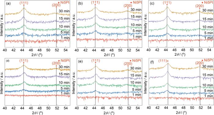
... 图3给出了磁控溅射参数不同的Ni5Pt合金薄膜的XRD谱,可见所有样品的谱中都出现了与(111)和(200)晶面对应的衍射峰,其中较为显著的(111)峰表明薄膜中的晶粒具有一定的择优取向.随着薄膜沉积时间的延长衍射峰强度逐渐提高,表明薄膜的结晶度提高,且晶体的择优取向更加明显,生长织构逐渐增强.需要指出的是,Ni-Pt合金体系中可能存在多种中间相(如NiPt、Ni3Pt、NiPt3等[25]),且这些相的衍射峰位与Ni5Pt相的(111)和(200)面峰位较为接近.为了准确判断薄膜的相结构,将样品的XRD谱与文献中的Ni5Pt薄膜的衍射谱比较.根据Ni-Pt二元合金的平衡相图[25],在Pt含量低于约20% (原子分数)的Ni富集区间体系处于稳定的面心立方(FCC)置换固溶体区域,不生成有序金属间化合物或第二相,据此判定薄膜中出现的衍射峰对应Ni5Pt相[9,16,19].此外,所有Ni5Pt薄膜的衍射峰均向低角度偏移,表明晶格常数有所增大,其原因可能是原子半径较大的Pt原子(0.139 nm)部分取代Ni原子(0.125 nm)进入晶格位置形成了置换型固溶体,使晶胞体积膨胀[14].这种在取向和温度不同的基底制备的薄膜相同的衍射峰偏移,进一步证实了成分主导的晶格膨胀机制[26].衍射峰展宽的原因有:在低温沉积薄膜中晶粒较小和在制备过程中薄膜出现一定程度的晶格畸变或微应变,特别是Pt原子非均匀分布或局部固溶在晶格内产生了弹性畸变场[27]. ...
Ni(Pt)-silicide contacts on CMOS devices: Impact of substrate nature and Pt concentration on the phase formation
1
2014
... 基于金属-半导体结的肖特基二极管(Schottky barrier diode, SBD)的正向压降较低、超高速响应和低功耗,得到了广泛的应用[1,2].SBD的整流特性和稳定性决定于其金属-半导体势垒,常用的势垒金属有Au[3]、Pt[4]、Ni[5]和Pd[6].但是,这些传统贵金属的热稳定性较低且功函数不可调.使用合金材料替代单一贵金属可精准调控势垒高度[7,8].镍铂(NiPt)合金的热稳定性较高且界面特性可调控,是主流势垒材料[9~11].制备NiPt基SBD用的是在Si基底磁控溅射的合金薄膜,将其热处理形成热稳定的NiPtSi势垒层可实现反向电流阻断[12].关于NiPt合金的研究,侧重于NiPt薄膜与Si形成的势垒高度[13]、热稳定性[11]以及高速退火工艺等方面[14].制备NiPt合金薄膜的工艺参数对SBD器件势垒层微结构和性能的影响尚须进一步深入研究[15~17].近年来,研究人员通过调控磁控溅射制备参数(如沉积时间、基底温度和沉积速率等)改善NiPt合金薄膜的表面粗糙度并调控残余应力[9,18,19].Shin等[18]用晶圆曲率法研究了xNi(1-x)Pt (0.02 < x < 0.81)薄膜的应力行为,发现富集Ni的样品对基底温度和沉积速率的变化极其敏感.随着基底温度的降低和沉积速率的提高,薄膜中的残余应力显著增大.Eiler等[19]分析了xNi(1-x)Pt (0.01 < x < 0.39)薄膜的杨氏模量和硬度的变化,发现随着沉积时间的延长表面粗糙度有所提高.Yang等[20]发现,基底取向对ZnO薄膜的表面粗糙度也有显著影响.取向不同的基底其原子排列不同,使在其上制备的薄膜原子的生长能力也不同.在Si(100)基底上制备的薄膜表面粗糙度略比Si(111)基底的低.Tsamouras和Galinski等[21,22]发现,随着基底温度的提高在其上制备的Pt薄膜表面粗糙度提高,因为基底原子的扩散增强和活化能增大.虽然有些工作研究了用不同工艺制备的NiPt合金薄膜的表面粗糙度和残余应力状态的变化,但是关于制备工艺参数不同的Ni5Pt合金薄膜的应力变化和薄膜表面质量仍缺少系统的研究[10,16,23],特别是亟需进一步揭示薄膜制备工艺参数对薄膜的残余应力和表面粗糙度的影响.鉴于此,本文在两种晶体取向的单晶硅基底上磁控溅射Ni5Pt合金薄膜,研究基底温度、沉积时间以及基底取向对薄膜的表面粗糙度和微观结构的影响,并根据薄膜的开裂行为以及残余应力分布建立薄膜开裂的判据. ...
NiPt salicide process improvement for 28 nm CMOS with Pt(10%) additive
2
2012
... 基于金属-半导体结的肖特基二极管(Schottky barrier diode, SBD)的正向压降较低、超高速响应和低功耗,得到了广泛的应用[1,2].SBD的整流特性和稳定性决定于其金属-半导体势垒,常用的势垒金属有Au[3]、Pt[4]、Ni[5]和Pd[6].但是,这些传统贵金属的热稳定性较低且功函数不可调.使用合金材料替代单一贵金属可精准调控势垒高度[7,8].镍铂(NiPt)合金的热稳定性较高且界面特性可调控,是主流势垒材料[9~11].制备NiPt基SBD用的是在Si基底磁控溅射的合金薄膜,将其热处理形成热稳定的NiPtSi势垒层可实现反向电流阻断[12].关于NiPt合金的研究,侧重于NiPt薄膜与Si形成的势垒高度[13]、热稳定性[11]以及高速退火工艺等方面[14].制备NiPt合金薄膜的工艺参数对SBD器件势垒层微结构和性能的影响尚须进一步深入研究[15~17].近年来,研究人员通过调控磁控溅射制备参数(如沉积时间、基底温度和沉积速率等)改善NiPt合金薄膜的表面粗糙度并调控残余应力[9,18,19].Shin等[18]用晶圆曲率法研究了xNi(1-x)Pt (0.02 < x < 0.81)薄膜的应力行为,发现富集Ni的样品对基底温度和沉积速率的变化极其敏感.随着基底温度的降低和沉积速率的提高,薄膜中的残余应力显著增大.Eiler等[19]分析了xNi(1-x)Pt (0.01 < x < 0.39)薄膜的杨氏模量和硬度的变化,发现随着沉积时间的延长表面粗糙度有所提高.Yang等[20]发现,基底取向对ZnO薄膜的表面粗糙度也有显著影响.取向不同的基底其原子排列不同,使在其上制备的薄膜原子的生长能力也不同.在Si(100)基底上制备的薄膜表面粗糙度略比Si(111)基底的低.Tsamouras和Galinski等[21,22]发现,随着基底温度的提高在其上制备的Pt薄膜表面粗糙度提高,因为基底原子的扩散增强和活化能增大.虽然有些工作研究了用不同工艺制备的NiPt合金薄膜的表面粗糙度和残余应力状态的变化,但是关于制备工艺参数不同的Ni5Pt合金薄膜的应力变化和薄膜表面质量仍缺少系统的研究[10,16,23],特别是亟需进一步揭示薄膜制备工艺参数对薄膜的残余应力和表面粗糙度的影响.鉴于此,本文在两种晶体取向的单晶硅基底上磁控溅射Ni5Pt合金薄膜,研究基底温度、沉积时间以及基底取向对薄膜的表面粗糙度和微观结构的影响,并根据薄膜的开裂行为以及残余应力分布建立薄膜开裂的判据. ...
... [11]以及高速退火工艺等方面[14].制备NiPt合金薄膜的工艺参数对SBD器件势垒层微结构和性能的影响尚须进一步深入研究[15~17].近年来,研究人员通过调控磁控溅射制备参数(如沉积时间、基底温度和沉积速率等)改善NiPt合金薄膜的表面粗糙度并调控残余应力[9,18,19].Shin等[18]用晶圆曲率法研究了xNi(1-x)Pt (0.02 < x < 0.81)薄膜的应力行为,发现富集Ni的样品对基底温度和沉积速率的变化极其敏感.随着基底温度的降低和沉积速率的提高,薄膜中的残余应力显著增大.Eiler等[19]分析了xNi(1-x)Pt (0.01 < x < 0.39)薄膜的杨氏模量和硬度的变化,发现随着沉积时间的延长表面粗糙度有所提高.Yang等[20]发现,基底取向对ZnO薄膜的表面粗糙度也有显著影响.取向不同的基底其原子排列不同,使在其上制备的薄膜原子的生长能力也不同.在Si(100)基底上制备的薄膜表面粗糙度略比Si(111)基底的低.Tsamouras和Galinski等[21,22]发现,随着基底温度的提高在其上制备的Pt薄膜表面粗糙度提高,因为基底原子的扩散增强和活化能增大.虽然有些工作研究了用不同工艺制备的NiPt合金薄膜的表面粗糙度和残余应力状态的变化,但是关于制备工艺参数不同的Ni5Pt合金薄膜的应力变化和薄膜表面质量仍缺少系统的研究[10,16,23],特别是亟需进一步揭示薄膜制备工艺参数对薄膜的残余应力和表面粗糙度的影响.鉴于此,本文在两种晶体取向的单晶硅基底上磁控溅射Ni5Pt合金薄膜,研究基底温度、沉积时间以及基底取向对薄膜的表面粗糙度和微观结构的影响,并根据薄膜的开裂行为以及残余应力分布建立薄膜开裂的判据. ...
Tailoring the electronic properties of nickel silicide by interfacial modification
1
2022
... 基于金属-半导体结的肖特基二极管(Schottky barrier diode, SBD)的正向压降较低、超高速响应和低功耗,得到了广泛的应用[1,2].SBD的整流特性和稳定性决定于其金属-半导体势垒,常用的势垒金属有Au[3]、Pt[4]、Ni[5]和Pd[6].但是,这些传统贵金属的热稳定性较低且功函数不可调.使用合金材料替代单一贵金属可精准调控势垒高度[7,8].镍铂(NiPt)合金的热稳定性较高且界面特性可调控,是主流势垒材料[9~11].制备NiPt基SBD用的是在Si基底磁控溅射的合金薄膜,将其热处理形成热稳定的NiPtSi势垒层可实现反向电流阻断[12].关于NiPt合金的研究,侧重于NiPt薄膜与Si形成的势垒高度[13]、热稳定性[11]以及高速退火工艺等方面[14].制备NiPt合金薄膜的工艺参数对SBD器件势垒层微结构和性能的影响尚须进一步深入研究[15~17].近年来,研究人员通过调控磁控溅射制备参数(如沉积时间、基底温度和沉积速率等)改善NiPt合金薄膜的表面粗糙度并调控残余应力[9,18,19].Shin等[18]用晶圆曲率法研究了xNi(1-x)Pt (0.02 < x < 0.81)薄膜的应力行为,发现富集Ni的样品对基底温度和沉积速率的变化极其敏感.随着基底温度的降低和沉积速率的提高,薄膜中的残余应力显著增大.Eiler等[19]分析了xNi(1-x)Pt (0.01 < x < 0.39)薄膜的杨氏模量和硬度的变化,发现随着沉积时间的延长表面粗糙度有所提高.Yang等[20]发现,基底取向对ZnO薄膜的表面粗糙度也有显著影响.取向不同的基底其原子排列不同,使在其上制备的薄膜原子的生长能力也不同.在Si(100)基底上制备的薄膜表面粗糙度略比Si(111)基底的低.Tsamouras和Galinski等[21,22]发现,随着基底温度的提高在其上制备的Pt薄膜表面粗糙度提高,因为基底原子的扩散增强和活化能增大.虽然有些工作研究了用不同工艺制备的NiPt合金薄膜的表面粗糙度和残余应力状态的变化,但是关于制备工艺参数不同的Ni5Pt合金薄膜的应力变化和薄膜表面质量仍缺少系统的研究[10,16,23],特别是亟需进一步揭示薄膜制备工艺参数对薄膜的残余应力和表面粗糙度的影响.鉴于此,本文在两种晶体取向的单晶硅基底上磁控溅射Ni5Pt合金薄膜,研究基底温度、沉积时间以及基底取向对薄膜的表面粗糙度和微观结构的影响,并根据薄膜的开裂行为以及残余应力分布建立薄膜开裂的判据. ...
Nickel silicide encroachment formation and characterization
1
2010
... 基于金属-半导体结的肖特基二极管(Schottky barrier diode, SBD)的正向压降较低、超高速响应和低功耗,得到了广泛的应用[1,2].SBD的整流特性和稳定性决定于其金属-半导体势垒,常用的势垒金属有Au[3]、Pt[4]、Ni[5]和Pd[6].但是,这些传统贵金属的热稳定性较低且功函数不可调.使用合金材料替代单一贵金属可精准调控势垒高度[7,8].镍铂(NiPt)合金的热稳定性较高且界面特性可调控,是主流势垒材料[9~11].制备NiPt基SBD用的是在Si基底磁控溅射的合金薄膜,将其热处理形成热稳定的NiPtSi势垒层可实现反向电流阻断[12].关于NiPt合金的研究,侧重于NiPt薄膜与Si形成的势垒高度[13]、热稳定性[11]以及高速退火工艺等方面[14].制备NiPt合金薄膜的工艺参数对SBD器件势垒层微结构和性能的影响尚须进一步深入研究[15~17].近年来,研究人员通过调控磁控溅射制备参数(如沉积时间、基底温度和沉积速率等)改善NiPt合金薄膜的表面粗糙度并调控残余应力[9,18,19].Shin等[18]用晶圆曲率法研究了xNi(1-x)Pt (0.02 < x < 0.81)薄膜的应力行为,发现富集Ni的样品对基底温度和沉积速率的变化极其敏感.随着基底温度的降低和沉积速率的提高,薄膜中的残余应力显著增大.Eiler等[19]分析了xNi(1-x)Pt (0.01 < x < 0.39)薄膜的杨氏模量和硬度的变化,发现随着沉积时间的延长表面粗糙度有所提高.Yang等[20]发现,基底取向对ZnO薄膜的表面粗糙度也有显著影响.取向不同的基底其原子排列不同,使在其上制备的薄膜原子的生长能力也不同.在Si(100)基底上制备的薄膜表面粗糙度略比Si(111)基底的低.Tsamouras和Galinski等[21,22]发现,随着基底温度的提高在其上制备的Pt薄膜表面粗糙度提高,因为基底原子的扩散增强和活化能增大.虽然有些工作研究了用不同工艺制备的NiPt合金薄膜的表面粗糙度和残余应力状态的变化,但是关于制备工艺参数不同的Ni5Pt合金薄膜的应力变化和薄膜表面质量仍缺少系统的研究[10,16,23],特别是亟需进一步揭示薄膜制备工艺参数对薄膜的残余应力和表面粗糙度的影响.鉴于此,本文在两种晶体取向的单晶硅基底上磁控溅射Ni5Pt合金薄膜,研究基底温度、沉积时间以及基底取向对薄膜的表面粗糙度和微观结构的影响,并根据薄膜的开裂行为以及残余应力分布建立薄膜开裂的判据. ...
Nanoscale effect on the formation of the amorphous Ni silicide by rapid thermal annealing from crystalline and pre-amorphized silicon
2
2024
... 基于金属-半导体结的肖特基二极管(Schottky barrier diode, SBD)的正向压降较低、超高速响应和低功耗,得到了广泛的应用[1,2].SBD的整流特性和稳定性决定于其金属-半导体势垒,常用的势垒金属有Au[3]、Pt[4]、Ni[5]和Pd[6].但是,这些传统贵金属的热稳定性较低且功函数不可调.使用合金材料替代单一贵金属可精准调控势垒高度[7,8].镍铂(NiPt)合金的热稳定性较高且界面特性可调控,是主流势垒材料[9~11].制备NiPt基SBD用的是在Si基底磁控溅射的合金薄膜,将其热处理形成热稳定的NiPtSi势垒层可实现反向电流阻断[12].关于NiPt合金的研究,侧重于NiPt薄膜与Si形成的势垒高度[13]、热稳定性[11]以及高速退火工艺等方面[14].制备NiPt合金薄膜的工艺参数对SBD器件势垒层微结构和性能的影响尚须进一步深入研究[15~17].近年来,研究人员通过调控磁控溅射制备参数(如沉积时间、基底温度和沉积速率等)改善NiPt合金薄膜的表面粗糙度并调控残余应力[9,18,19].Shin等[18]用晶圆曲率法研究了xNi(1-x)Pt (0.02 < x < 0.81)薄膜的应力行为,发现富集Ni的样品对基底温度和沉积速率的变化极其敏感.随着基底温度的降低和沉积速率的提高,薄膜中的残余应力显著增大.Eiler等[19]分析了xNi(1-x)Pt (0.01 < x < 0.39)薄膜的杨氏模量和硬度的变化,发现随着沉积时间的延长表面粗糙度有所提高.Yang等[20]发现,基底取向对ZnO薄膜的表面粗糙度也有显著影响.取向不同的基底其原子排列不同,使在其上制备的薄膜原子的生长能力也不同.在Si(100)基底上制备的薄膜表面粗糙度略比Si(111)基底的低.Tsamouras和Galinski等[21,22]发现,随着基底温度的提高在其上制备的Pt薄膜表面粗糙度提高,因为基底原子的扩散增强和活化能增大.虽然有些工作研究了用不同工艺制备的NiPt合金薄膜的表面粗糙度和残余应力状态的变化,但是关于制备工艺参数不同的Ni5Pt合金薄膜的应力变化和薄膜表面质量仍缺少系统的研究[10,16,23],特别是亟需进一步揭示薄膜制备工艺参数对薄膜的残余应力和表面粗糙度的影响.鉴于此,本文在两种晶体取向的单晶硅基底上磁控溅射Ni5Pt合金薄膜,研究基底温度、沉积时间以及基底取向对薄膜的表面粗糙度和微观结构的影响,并根据薄膜的开裂行为以及残余应力分布建立薄膜开裂的判据. ...
... 图3给出了磁控溅射参数不同的Ni5Pt合金薄膜的XRD谱,可见所有样品的谱中都出现了与(111)和(200)晶面对应的衍射峰,其中较为显著的(111)峰表明薄膜中的晶粒具有一定的择优取向.随着薄膜沉积时间的延长衍射峰强度逐渐提高,表明薄膜的结晶度提高,且晶体的择优取向更加明显,生长织构逐渐增强.需要指出的是,Ni-Pt合金体系中可能存在多种中间相(如NiPt、Ni3Pt、NiPt3等[25]),且这些相的衍射峰位与Ni5Pt相的(111)和(200)面峰位较为接近.为了准确判断薄膜的相结构,将样品的XRD谱与文献中的Ni5Pt薄膜的衍射谱比较.根据Ni-Pt二元合金的平衡相图[25],在Pt含量低于约20% (原子分数)的Ni富集区间体系处于稳定的面心立方(FCC)置换固溶体区域,不生成有序金属间化合物或第二相,据此判定薄膜中出现的衍射峰对应Ni5Pt相[9,16,19].此外,所有Ni5Pt薄膜的衍射峰均向低角度偏移,表明晶格常数有所增大,其原因可能是原子半径较大的Pt原子(0.139 nm)部分取代Ni原子(0.125 nm)进入晶格位置形成了置换型固溶体,使晶胞体积膨胀[14].这种在取向和温度不同的基底制备的薄膜相同的衍射峰偏移,进一步证实了成分主导的晶格膨胀机制[26].衍射峰展宽的原因有:在低温沉积薄膜中晶粒较小和在制备过程中薄膜出现一定程度的晶格畸变或微应变,特别是Pt原子非均匀分布或局部固溶在晶格内产生了弹性畸变场[27]. ...
Research progress on precious metal sputtering target
1
2021
... 基于金属-半导体结的肖特基二极管(Schottky barrier diode, SBD)的正向压降较低、超高速响应和低功耗,得到了广泛的应用[1,2].SBD的整流特性和稳定性决定于其金属-半导体势垒,常用的势垒金属有Au[3]、Pt[4]、Ni[5]和Pd[6].但是,这些传统贵金属的热稳定性较低且功函数不可调.使用合金材料替代单一贵金属可精准调控势垒高度[7,8].镍铂(NiPt)合金的热稳定性较高且界面特性可调控,是主流势垒材料[9~11].制备NiPt基SBD用的是在Si基底磁控溅射的合金薄膜,将其热处理形成热稳定的NiPtSi势垒层可实现反向电流阻断[12].关于NiPt合金的研究,侧重于NiPt薄膜与Si形成的势垒高度[13]、热稳定性[11]以及高速退火工艺等方面[14].制备NiPt合金薄膜的工艺参数对SBD器件势垒层微结构和性能的影响尚须进一步深入研究[15~17].近年来,研究人员通过调控磁控溅射制备参数(如沉积时间、基底温度和沉积速率等)改善NiPt合金薄膜的表面粗糙度并调控残余应力[9,18,19].Shin等[18]用晶圆曲率法研究了xNi(1-x)Pt (0.02 < x < 0.81)薄膜的应力行为,发现富集Ni的样品对基底温度和沉积速率的变化极其敏感.随着基底温度的降低和沉积速率的提高,薄膜中的残余应力显著增大.Eiler等[19]分析了xNi(1-x)Pt (0.01 < x < 0.39)薄膜的杨氏模量和硬度的变化,发现随着沉积时间的延长表面粗糙度有所提高.Yang等[20]发现,基底取向对ZnO薄膜的表面粗糙度也有显著影响.取向不同的基底其原子排列不同,使在其上制备的薄膜原子的生长能力也不同.在Si(100)基底上制备的薄膜表面粗糙度略比Si(111)基底的低.Tsamouras和Galinski等[21,22]发现,随着基底温度的提高在其上制备的Pt薄膜表面粗糙度提高,因为基底原子的扩散增强和活化能增大.虽然有些工作研究了用不同工艺制备的NiPt合金薄膜的表面粗糙度和残余应力状态的变化,但是关于制备工艺参数不同的Ni5Pt合金薄膜的应力变化和薄膜表面质量仍缺少系统的研究[10,16,23],特别是亟需进一步揭示薄膜制备工艺参数对薄膜的残余应力和表面粗糙度的影响.鉴于此,本文在两种晶体取向的单晶硅基底上磁控溅射Ni5Pt合金薄膜,研究基底温度、沉积时间以及基底取向对薄膜的表面粗糙度和微观结构的影响,并根据薄膜的开裂行为以及残余应力分布建立薄膜开裂的判据. ...
贵金属溅射靶材的研究进展
1
2021
... 基于金属-半导体结的肖特基二极管(Schottky barrier diode, SBD)的正向压降较低、超高速响应和低功耗,得到了广泛的应用[1,2].SBD的整流特性和稳定性决定于其金属-半导体势垒,常用的势垒金属有Au[3]、Pt[4]、Ni[5]和Pd[6].但是,这些传统贵金属的热稳定性较低且功函数不可调.使用合金材料替代单一贵金属可精准调控势垒高度[7,8].镍铂(NiPt)合金的热稳定性较高且界面特性可调控,是主流势垒材料[9~11].制备NiPt基SBD用的是在Si基底磁控溅射的合金薄膜,将其热处理形成热稳定的NiPtSi势垒层可实现反向电流阻断[12].关于NiPt合金的研究,侧重于NiPt薄膜与Si形成的势垒高度[13]、热稳定性[11]以及高速退火工艺等方面[14].制备NiPt合金薄膜的工艺参数对SBD器件势垒层微结构和性能的影响尚须进一步深入研究[15~17].近年来,研究人员通过调控磁控溅射制备参数(如沉积时间、基底温度和沉积速率等)改善NiPt合金薄膜的表面粗糙度并调控残余应力[9,18,19].Shin等[18]用晶圆曲率法研究了xNi(1-x)Pt (0.02 < x < 0.81)薄膜的应力行为,发现富集Ni的样品对基底温度和沉积速率的变化极其敏感.随着基底温度的降低和沉积速率的提高,薄膜中的残余应力显著增大.Eiler等[19]分析了xNi(1-x)Pt (0.01 < x < 0.39)薄膜的杨氏模量和硬度的变化,发现随着沉积时间的延长表面粗糙度有所提高.Yang等[20]发现,基底取向对ZnO薄膜的表面粗糙度也有显著影响.取向不同的基底其原子排列不同,使在其上制备的薄膜原子的生长能力也不同.在Si(100)基底上制备的薄膜表面粗糙度略比Si(111)基底的低.Tsamouras和Galinski等[21,22]发现,随着基底温度的提高在其上制备的Pt薄膜表面粗糙度提高,因为基底原子的扩散增强和活化能增大.虽然有些工作研究了用不同工艺制备的NiPt合金薄膜的表面粗糙度和残余应力状态的变化,但是关于制备工艺参数不同的Ni5Pt合金薄膜的应力变化和薄膜表面质量仍缺少系统的研究[10,16,23],特别是亟需进一步揭示薄膜制备工艺参数对薄膜的残余应力和表面粗糙度的影响.鉴于此,本文在两种晶体取向的单晶硅基底上磁控溅射Ni5Pt合金薄膜,研究基底温度、沉积时间以及基底取向对薄膜的表面粗糙度和微观结构的影响,并根据薄膜的开裂行为以及残余应力分布建立薄膜开裂的判据. ...
Microstructure evolution and magnetic properties of Ni-5Pt alloy during cold rolling
2
2020
... 基于金属-半导体结的肖特基二极管(Schottky barrier diode, SBD)的正向压降较低、超高速响应和低功耗,得到了广泛的应用[1,2].SBD的整流特性和稳定性决定于其金属-半导体势垒,常用的势垒金属有Au[3]、Pt[4]、Ni[5]和Pd[6].但是,这些传统贵金属的热稳定性较低且功函数不可调.使用合金材料替代单一贵金属可精准调控势垒高度[7,8].镍铂(NiPt)合金的热稳定性较高且界面特性可调控,是主流势垒材料[9~11].制备NiPt基SBD用的是在Si基底磁控溅射的合金薄膜,将其热处理形成热稳定的NiPtSi势垒层可实现反向电流阻断[12].关于NiPt合金的研究,侧重于NiPt薄膜与Si形成的势垒高度[13]、热稳定性[11]以及高速退火工艺等方面[14].制备NiPt合金薄膜的工艺参数对SBD器件势垒层微结构和性能的影响尚须进一步深入研究[15~17].近年来,研究人员通过调控磁控溅射制备参数(如沉积时间、基底温度和沉积速率等)改善NiPt合金薄膜的表面粗糙度并调控残余应力[9,18,19].Shin等[18]用晶圆曲率法研究了xNi(1-x)Pt (0.02 < x < 0.81)薄膜的应力行为,发现富集Ni的样品对基底温度和沉积速率的变化极其敏感.随着基底温度的降低和沉积速率的提高,薄膜中的残余应力显著增大.Eiler等[19]分析了xNi(1-x)Pt (0.01 < x < 0.39)薄膜的杨氏模量和硬度的变化,发现随着沉积时间的延长表面粗糙度有所提高.Yang等[20]发现,基底取向对ZnO薄膜的表面粗糙度也有显著影响.取向不同的基底其原子排列不同,使在其上制备的薄膜原子的生长能力也不同.在Si(100)基底上制备的薄膜表面粗糙度略比Si(111)基底的低.Tsamouras和Galinski等[21,22]发现,随着基底温度的提高在其上制备的Pt薄膜表面粗糙度提高,因为基底原子的扩散增强和活化能增大.虽然有些工作研究了用不同工艺制备的NiPt合金薄膜的表面粗糙度和残余应力状态的变化,但是关于制备工艺参数不同的Ni5Pt合金薄膜的应力变化和薄膜表面质量仍缺少系统的研究[10,16,23],特别是亟需进一步揭示薄膜制备工艺参数对薄膜的残余应力和表面粗糙度的影响.鉴于此,本文在两种晶体取向的单晶硅基底上磁控溅射Ni5Pt合金薄膜,研究基底温度、沉积时间以及基底取向对薄膜的表面粗糙度和微观结构的影响,并根据薄膜的开裂行为以及残余应力分布建立薄膜开裂的判据. ...
... 图3给出了磁控溅射参数不同的Ni5Pt合金薄膜的XRD谱,可见所有样品的谱中都出现了与(111)和(200)晶面对应的衍射峰,其中较为显著的(111)峰表明薄膜中的晶粒具有一定的择优取向.随着薄膜沉积时间的延长衍射峰强度逐渐提高,表明薄膜的结晶度提高,且晶体的择优取向更加明显,生长织构逐渐增强.需要指出的是,Ni-Pt合金体系中可能存在多种中间相(如NiPt、Ni3Pt、NiPt3等[25]),且这些相的衍射峰位与Ni5Pt相的(111)和(200)面峰位较为接近.为了准确判断薄膜的相结构,将样品的XRD谱与文献中的Ni5Pt薄膜的衍射谱比较.根据Ni-Pt二元合金的平衡相图[25],在Pt含量低于约20% (原子分数)的Ni富集区间体系处于稳定的面心立方(FCC)置换固溶体区域,不生成有序金属间化合物或第二相,据此判定薄膜中出现的衍射峰对应Ni5Pt相[9,16,19].此外,所有Ni5Pt薄膜的衍射峰均向低角度偏移,表明晶格常数有所增大,其原因可能是原子半径较大的Pt原子(0.139 nm)部分取代Ni原子(0.125 nm)进入晶格位置形成了置换型固溶体,使晶胞体积膨胀[14].这种在取向和温度不同的基底制备的薄膜相同的衍射峰偏移,进一步证实了成分主导的晶格膨胀机制[26].衍射峰展宽的原因有:在低温沉积薄膜中晶粒较小和在制备过程中薄膜出现一定程度的晶格畸变或微应变,特别是Pt原子非均匀分布或局部固溶在晶格内产生了弹性畸变场[27]. ...
冷轧过程中NiPt5合金的结构演变及磁性能
2
2020
... 基于金属-半导体结的肖特基二极管(Schottky barrier diode, SBD)的正向压降较低、超高速响应和低功耗,得到了广泛的应用[1,2].SBD的整流特性和稳定性决定于其金属-半导体势垒,常用的势垒金属有Au[3]、Pt[4]、Ni[5]和Pd[6].但是,这些传统贵金属的热稳定性较低且功函数不可调.使用合金材料替代单一贵金属可精准调控势垒高度[7,8].镍铂(NiPt)合金的热稳定性较高且界面特性可调控,是主流势垒材料[9~11].制备NiPt基SBD用的是在Si基底磁控溅射的合金薄膜,将其热处理形成热稳定的NiPtSi势垒层可实现反向电流阻断[12].关于NiPt合金的研究,侧重于NiPt薄膜与Si形成的势垒高度[13]、热稳定性[11]以及高速退火工艺等方面[14].制备NiPt合金薄膜的工艺参数对SBD器件势垒层微结构和性能的影响尚须进一步深入研究[15~17].近年来,研究人员通过调控磁控溅射制备参数(如沉积时间、基底温度和沉积速率等)改善NiPt合金薄膜的表面粗糙度并调控残余应力[9,18,19].Shin等[18]用晶圆曲率法研究了xNi(1-x)Pt (0.02 < x < 0.81)薄膜的应力行为,发现富集Ni的样品对基底温度和沉积速率的变化极其敏感.随着基底温度的降低和沉积速率的提高,薄膜中的残余应力显著增大.Eiler等[19]分析了xNi(1-x)Pt (0.01 < x < 0.39)薄膜的杨氏模量和硬度的变化,发现随着沉积时间的延长表面粗糙度有所提高.Yang等[20]发现,基底取向对ZnO薄膜的表面粗糙度也有显著影响.取向不同的基底其原子排列不同,使在其上制备的薄膜原子的生长能力也不同.在Si(100)基底上制备的薄膜表面粗糙度略比Si(111)基底的低.Tsamouras和Galinski等[21,22]发现,随着基底温度的提高在其上制备的Pt薄膜表面粗糙度提高,因为基底原子的扩散增强和活化能增大.虽然有些工作研究了用不同工艺制备的NiPt合金薄膜的表面粗糙度和残余应力状态的变化,但是关于制备工艺参数不同的Ni5Pt合金薄膜的应力变化和薄膜表面质量仍缺少系统的研究[10,16,23],特别是亟需进一步揭示薄膜制备工艺参数对薄膜的残余应力和表面粗糙度的影响.鉴于此,本文在两种晶体取向的单晶硅基底上磁控溅射Ni5Pt合金薄膜,研究基底温度、沉积时间以及基底取向对薄膜的表面粗糙度和微观结构的影响,并根据薄膜的开裂行为以及残余应力分布建立薄膜开裂的判据. ...
... 图3给出了磁控溅射参数不同的Ni5Pt合金薄膜的XRD谱,可见所有样品的谱中都出现了与(111)和(200)晶面对应的衍射峰,其中较为显著的(111)峰表明薄膜中的晶粒具有一定的择优取向.随着薄膜沉积时间的延长衍射峰强度逐渐提高,表明薄膜的结晶度提高,且晶体的择优取向更加明显,生长织构逐渐增强.需要指出的是,Ni-Pt合金体系中可能存在多种中间相(如NiPt、Ni3Pt、NiPt3等[25]),且这些相的衍射峰位与Ni5Pt相的(111)和(200)面峰位较为接近.为了准确判断薄膜的相结构,将样品的XRD谱与文献中的Ni5Pt薄膜的衍射谱比较.根据Ni-Pt二元合金的平衡相图[25],在Pt含量低于约20% (原子分数)的Ni富集区间体系处于稳定的面心立方(FCC)置换固溶体区域,不生成有序金属间化合物或第二相,据此判定薄膜中出现的衍射峰对应Ni5Pt相[9,16,19].此外,所有Ni5Pt薄膜的衍射峰均向低角度偏移,表明晶格常数有所增大,其原因可能是原子半径较大的Pt原子(0.139 nm)部分取代Ni原子(0.125 nm)进入晶格位置形成了置换型固溶体,使晶胞体积膨胀[14].这种在取向和温度不同的基底制备的薄膜相同的衍射峰偏移,进一步证实了成分主导的晶格膨胀机制[26].衍射峰展宽的原因有:在低温沉积薄膜中晶粒较小和在制备过程中薄膜出现一定程度的晶格畸变或微应变,特别是Pt原子非均匀分布或局部固溶在晶格内产生了弹性畸变场[27]. ...
Hot deformation behavior and hot processing maps of NiPt15 alloys
1
2021
... 基于金属-半导体结的肖特基二极管(Schottky barrier diode, SBD)的正向压降较低、超高速响应和低功耗,得到了广泛的应用[1,2].SBD的整流特性和稳定性决定于其金属-半导体势垒,常用的势垒金属有Au[3]、Pt[4]、Ni[5]和Pd[6].但是,这些传统贵金属的热稳定性较低且功函数不可调.使用合金材料替代单一贵金属可精准调控势垒高度[7,8].镍铂(NiPt)合金的热稳定性较高且界面特性可调控,是主流势垒材料[9~11].制备NiPt基SBD用的是在Si基底磁控溅射的合金薄膜,将其热处理形成热稳定的NiPtSi势垒层可实现反向电流阻断[12].关于NiPt合金的研究,侧重于NiPt薄膜与Si形成的势垒高度[13]、热稳定性[11]以及高速退火工艺等方面[14].制备NiPt合金薄膜的工艺参数对SBD器件势垒层微结构和性能的影响尚须进一步深入研究[15~17].近年来,研究人员通过调控磁控溅射制备参数(如沉积时间、基底温度和沉积速率等)改善NiPt合金薄膜的表面粗糙度并调控残余应力[9,18,19].Shin等[18]用晶圆曲率法研究了xNi(1-x)Pt (0.02 < x < 0.81)薄膜的应力行为,发现富集Ni的样品对基底温度和沉积速率的变化极其敏感.随着基底温度的降低和沉积速率的提高,薄膜中的残余应力显著增大.Eiler等[19]分析了xNi(1-x)Pt (0.01 < x < 0.39)薄膜的杨氏模量和硬度的变化,发现随着沉积时间的延长表面粗糙度有所提高.Yang等[20]发现,基底取向对ZnO薄膜的表面粗糙度也有显著影响.取向不同的基底其原子排列不同,使在其上制备的薄膜原子的生长能力也不同.在Si(100)基底上制备的薄膜表面粗糙度略比Si(111)基底的低.Tsamouras和Galinski等[21,22]发现,随着基底温度的提高在其上制备的Pt薄膜表面粗糙度提高,因为基底原子的扩散增强和活化能增大.虽然有些工作研究了用不同工艺制备的NiPt合金薄膜的表面粗糙度和残余应力状态的变化,但是关于制备工艺参数不同的Ni5Pt合金薄膜的应力变化和薄膜表面质量仍缺少系统的研究[10,16,23],特别是亟需进一步揭示薄膜制备工艺参数对薄膜的残余应力和表面粗糙度的影响.鉴于此,本文在两种晶体取向的单晶硅基底上磁控溅射Ni5Pt合金薄膜,研究基底温度、沉积时间以及基底取向对薄膜的表面粗糙度和微观结构的影响,并根据薄膜的开裂行为以及残余应力分布建立薄膜开裂的判据. ...
NiPt15合金热变形行为及热加工图研究
1
2021
... 基于金属-半导体结的肖特基二极管(Schottky barrier diode, SBD)的正向压降较低、超高速响应和低功耗,得到了广泛的应用[1,2].SBD的整流特性和稳定性决定于其金属-半导体势垒,常用的势垒金属有Au[3]、Pt[4]、Ni[5]和Pd[6].但是,这些传统贵金属的热稳定性较低且功函数不可调.使用合金材料替代单一贵金属可精准调控势垒高度[7,8].镍铂(NiPt)合金的热稳定性较高且界面特性可调控,是主流势垒材料[9~11].制备NiPt基SBD用的是在Si基底磁控溅射的合金薄膜,将其热处理形成热稳定的NiPtSi势垒层可实现反向电流阻断[12].关于NiPt合金的研究,侧重于NiPt薄膜与Si形成的势垒高度[13]、热稳定性[11]以及高速退火工艺等方面[14].制备NiPt合金薄膜的工艺参数对SBD器件势垒层微结构和性能的影响尚须进一步深入研究[15~17].近年来,研究人员通过调控磁控溅射制备参数(如沉积时间、基底温度和沉积速率等)改善NiPt合金薄膜的表面粗糙度并调控残余应力[9,18,19].Shin等[18]用晶圆曲率法研究了xNi(1-x)Pt (0.02 < x < 0.81)薄膜的应力行为,发现富集Ni的样品对基底温度和沉积速率的变化极其敏感.随着基底温度的降低和沉积速率的提高,薄膜中的残余应力显著增大.Eiler等[19]分析了xNi(1-x)Pt (0.01 < x < 0.39)薄膜的杨氏模量和硬度的变化,发现随着沉积时间的延长表面粗糙度有所提高.Yang等[20]发现,基底取向对ZnO薄膜的表面粗糙度也有显著影响.取向不同的基底其原子排列不同,使在其上制备的薄膜原子的生长能力也不同.在Si(100)基底上制备的薄膜表面粗糙度略比Si(111)基底的低.Tsamouras和Galinski等[21,22]发现,随着基底温度的提高在其上制备的Pt薄膜表面粗糙度提高,因为基底原子的扩散增强和活化能增大.虽然有些工作研究了用不同工艺制备的NiPt合金薄膜的表面粗糙度和残余应力状态的变化,但是关于制备工艺参数不同的Ni5Pt合金薄膜的应力变化和薄膜表面质量仍缺少系统的研究[10,16,23],特别是亟需进一步揭示薄膜制备工艺参数对薄膜的残余应力和表面粗糙度的影响.鉴于此,本文在两种晶体取向的单晶硅基底上磁控溅射Ni5Pt合金薄膜,研究基底温度、沉积时间以及基底取向对薄膜的表面粗糙度和微观结构的影响,并根据薄膜的开裂行为以及残余应力分布建立薄膜开裂的判据. ...
In situ stress measurement during electrodeposition of Ni x Pt1- x alloys
2
2012
... 基于金属-半导体结的肖特基二极管(Schottky barrier diode, SBD)的正向压降较低、超高速响应和低功耗,得到了广泛的应用[1,2].SBD的整流特性和稳定性决定于其金属-半导体势垒,常用的势垒金属有Au[3]、Pt[4]、Ni[5]和Pd[6].但是,这些传统贵金属的热稳定性较低且功函数不可调.使用合金材料替代单一贵金属可精准调控势垒高度[7,8].镍铂(NiPt)合金的热稳定性较高且界面特性可调控,是主流势垒材料[9~11].制备NiPt基SBD用的是在Si基底磁控溅射的合金薄膜,将其热处理形成热稳定的NiPtSi势垒层可实现反向电流阻断[12].关于NiPt合金的研究,侧重于NiPt薄膜与Si形成的势垒高度[13]、热稳定性[11]以及高速退火工艺等方面[14].制备NiPt合金薄膜的工艺参数对SBD器件势垒层微结构和性能的影响尚须进一步深入研究[15~17].近年来,研究人员通过调控磁控溅射制备参数(如沉积时间、基底温度和沉积速率等)改善NiPt合金薄膜的表面粗糙度并调控残余应力[9,18,19].Shin等[18]用晶圆曲率法研究了xNi(1-x)Pt (0.02 < x < 0.81)薄膜的应力行为,发现富集Ni的样品对基底温度和沉积速率的变化极其敏感.随着基底温度的降低和沉积速率的提高,薄膜中的残余应力显著增大.Eiler等[19]分析了xNi(1-x)Pt (0.01 < x < 0.39)薄膜的杨氏模量和硬度的变化,发现随着沉积时间的延长表面粗糙度有所提高.Yang等[20]发现,基底取向对ZnO薄膜的表面粗糙度也有显著影响.取向不同的基底其原子排列不同,使在其上制备的薄膜原子的生长能力也不同.在Si(100)基底上制备的薄膜表面粗糙度略比Si(111)基底的低.Tsamouras和Galinski等[21,22]发现,随着基底温度的提高在其上制备的Pt薄膜表面粗糙度提高,因为基底原子的扩散增强和活化能增大.虽然有些工作研究了用不同工艺制备的NiPt合金薄膜的表面粗糙度和残余应力状态的变化,但是关于制备工艺参数不同的Ni5Pt合金薄膜的应力变化和薄膜表面质量仍缺少系统的研究[10,16,23],特别是亟需进一步揭示薄膜制备工艺参数对薄膜的残余应力和表面粗糙度的影响.鉴于此,本文在两种晶体取向的单晶硅基底上磁控溅射Ni5Pt合金薄膜,研究基底温度、沉积时间以及基底取向对薄膜的表面粗糙度和微观结构的影响,并根据薄膜的开裂行为以及残余应力分布建立薄膜开裂的判据. ...
... [18]用晶圆曲率法研究了xNi(1-x)Pt (0.02 < x < 0.81)薄膜的应力行为,发现富集Ni的样品对基底温度和沉积速率的变化极其敏感.随着基底温度的降低和沉积速率的提高,薄膜中的残余应力显著增大.Eiler等[19]分析了xNi(1-x)Pt (0.01 < x < 0.39)薄膜的杨氏模量和硬度的变化,发现随着沉积时间的延长表面粗糙度有所提高.Yang等[20]发现,基底取向对ZnO薄膜的表面粗糙度也有显著影响.取向不同的基底其原子排列不同,使在其上制备的薄膜原子的生长能力也不同.在Si(100)基底上制备的薄膜表面粗糙度略比Si(111)基底的低.Tsamouras和Galinski等[21,22]发现,随着基底温度的提高在其上制备的Pt薄膜表面粗糙度提高,因为基底原子的扩散增强和活化能增大.虽然有些工作研究了用不同工艺制备的NiPt合金薄膜的表面粗糙度和残余应力状态的变化,但是关于制备工艺参数不同的Ni5Pt合金薄膜的应力变化和薄膜表面质量仍缺少系统的研究[10,16,23],特别是亟需进一步揭示薄膜制备工艺参数对薄膜的残余应力和表面粗糙度的影响.鉴于此,本文在两种晶体取向的单晶硅基底上磁控溅射Ni5Pt合金薄膜,研究基底温度、沉积时间以及基底取向对薄膜的表面粗糙度和微观结构的影响,并根据薄膜的开裂行为以及残余应力分布建立薄膜开裂的判据. ...
Tailoring magnetic and mechanical properties of mesoporous single-phase Ni-Pt films by electrodeposition
3
2020
... 基于金属-半导体结的肖特基二极管(Schottky barrier diode, SBD)的正向压降较低、超高速响应和低功耗,得到了广泛的应用[1,2].SBD的整流特性和稳定性决定于其金属-半导体势垒,常用的势垒金属有Au[3]、Pt[4]、Ni[5]和Pd[6].但是,这些传统贵金属的热稳定性较低且功函数不可调.使用合金材料替代单一贵金属可精准调控势垒高度[7,8].镍铂(NiPt)合金的热稳定性较高且界面特性可调控,是主流势垒材料[9~11].制备NiPt基SBD用的是在Si基底磁控溅射的合金薄膜,将其热处理形成热稳定的NiPtSi势垒层可实现反向电流阻断[12].关于NiPt合金的研究,侧重于NiPt薄膜与Si形成的势垒高度[13]、热稳定性[11]以及高速退火工艺等方面[14].制备NiPt合金薄膜的工艺参数对SBD器件势垒层微结构和性能的影响尚须进一步深入研究[15~17].近年来,研究人员通过调控磁控溅射制备参数(如沉积时间、基底温度和沉积速率等)改善NiPt合金薄膜的表面粗糙度并调控残余应力[9,18,19].Shin等[18]用晶圆曲率法研究了xNi(1-x)Pt (0.02 < x < 0.81)薄膜的应力行为,发现富集Ni的样品对基底温度和沉积速率的变化极其敏感.随着基底温度的降低和沉积速率的提高,薄膜中的残余应力显著增大.Eiler等[19]分析了xNi(1-x)Pt (0.01 < x < 0.39)薄膜的杨氏模量和硬度的变化,发现随着沉积时间的延长表面粗糙度有所提高.Yang等[20]发现,基底取向对ZnO薄膜的表面粗糙度也有显著影响.取向不同的基底其原子排列不同,使在其上制备的薄膜原子的生长能力也不同.在Si(100)基底上制备的薄膜表面粗糙度略比Si(111)基底的低.Tsamouras和Galinski等[21,22]发现,随着基底温度的提高在其上制备的Pt薄膜表面粗糙度提高,因为基底原子的扩散增强和活化能增大.虽然有些工作研究了用不同工艺制备的NiPt合金薄膜的表面粗糙度和残余应力状态的变化,但是关于制备工艺参数不同的Ni5Pt合金薄膜的应力变化和薄膜表面质量仍缺少系统的研究[10,16,23],特别是亟需进一步揭示薄膜制备工艺参数对薄膜的残余应力和表面粗糙度的影响.鉴于此,本文在两种晶体取向的单晶硅基底上磁控溅射Ni5Pt合金薄膜,研究基底温度、沉积时间以及基底取向对薄膜的表面粗糙度和微观结构的影响,并根据薄膜的开裂行为以及残余应力分布建立薄膜开裂的判据. ...
... [19]分析了xNi(1-x)Pt (0.01 < x < 0.39)薄膜的杨氏模量和硬度的变化,发现随着沉积时间的延长表面粗糙度有所提高.Yang等[20]发现,基底取向对ZnO薄膜的表面粗糙度也有显著影响.取向不同的基底其原子排列不同,使在其上制备的薄膜原子的生长能力也不同.在Si(100)基底上制备的薄膜表面粗糙度略比Si(111)基底的低.Tsamouras和Galinski等[21,22]发现,随着基底温度的提高在其上制备的Pt薄膜表面粗糙度提高,因为基底原子的扩散增强和活化能增大.虽然有些工作研究了用不同工艺制备的NiPt合金薄膜的表面粗糙度和残余应力状态的变化,但是关于制备工艺参数不同的Ni5Pt合金薄膜的应力变化和薄膜表面质量仍缺少系统的研究[10,16,23],特别是亟需进一步揭示薄膜制备工艺参数对薄膜的残余应力和表面粗糙度的影响.鉴于此,本文在两种晶体取向的单晶硅基底上磁控溅射Ni5Pt合金薄膜,研究基底温度、沉积时间以及基底取向对薄膜的表面粗糙度和微观结构的影响,并根据薄膜的开裂行为以及残余应力分布建立薄膜开裂的判据. ...
... 图3给出了磁控溅射参数不同的Ni5Pt合金薄膜的XRD谱,可见所有样品的谱中都出现了与(111)和(200)晶面对应的衍射峰,其中较为显著的(111)峰表明薄膜中的晶粒具有一定的择优取向.随着薄膜沉积时间的延长衍射峰强度逐渐提高,表明薄膜的结晶度提高,且晶体的择优取向更加明显,生长织构逐渐增强.需要指出的是,Ni-Pt合金体系中可能存在多种中间相(如NiPt、Ni3Pt、NiPt3等[25]),且这些相的衍射峰位与Ni5Pt相的(111)和(200)面峰位较为接近.为了准确判断薄膜的相结构,将样品的XRD谱与文献中的Ni5Pt薄膜的衍射谱比较.根据Ni-Pt二元合金的平衡相图[25],在Pt含量低于约20% (原子分数)的Ni富集区间体系处于稳定的面心立方(FCC)置换固溶体区域,不生成有序金属间化合物或第二相,据此判定薄膜中出现的衍射峰对应Ni5Pt相[9,16,19].此外,所有Ni5Pt薄膜的衍射峰均向低角度偏移,表明晶格常数有所增大,其原因可能是原子半径较大的Pt原子(0.139 nm)部分取代Ni原子(0.125 nm)进入晶格位置形成了置换型固溶体,使晶胞体积膨胀[14].这种在取向和温度不同的基底制备的薄膜相同的衍射峰偏移,进一步证实了成分主导的晶格膨胀机制[26].衍射峰展宽的原因有:在低温沉积薄膜中晶粒较小和在制备过程中薄膜出现一定程度的晶格畸变或微应变,特别是Pt原子非均匀分布或局部固溶在晶格内产生了弹性畸变场[27]. ...
Morphology, electrical and optical properties of magnetron sputtered porous ZnO thin films on Si(100) and Si(111) substrates
1
2020
... 基于金属-半导体结的肖特基二极管(Schottky barrier diode, SBD)的正向压降较低、超高速响应和低功耗,得到了广泛的应用[1,2].SBD的整流特性和稳定性决定于其金属-半导体势垒,常用的势垒金属有Au[3]、Pt[4]、Ni[5]和Pd[6].但是,这些传统贵金属的热稳定性较低且功函数不可调.使用合金材料替代单一贵金属可精准调控势垒高度[7,8].镍铂(NiPt)合金的热稳定性较高且界面特性可调控,是主流势垒材料[9~11].制备NiPt基SBD用的是在Si基底磁控溅射的合金薄膜,将其热处理形成热稳定的NiPtSi势垒层可实现反向电流阻断[12].关于NiPt合金的研究,侧重于NiPt薄膜与Si形成的势垒高度[13]、热稳定性[11]以及高速退火工艺等方面[14].制备NiPt合金薄膜的工艺参数对SBD器件势垒层微结构和性能的影响尚须进一步深入研究[15~17].近年来,研究人员通过调控磁控溅射制备参数(如沉积时间、基底温度和沉积速率等)改善NiPt合金薄膜的表面粗糙度并调控残余应力[9,18,19].Shin等[18]用晶圆曲率法研究了xNi(1-x)Pt (0.02 < x < 0.81)薄膜的应力行为,发现富集Ni的样品对基底温度和沉积速率的变化极其敏感.随着基底温度的降低和沉积速率的提高,薄膜中的残余应力显著增大.Eiler等[19]分析了xNi(1-x)Pt (0.01 < x < 0.39)薄膜的杨氏模量和硬度的变化,发现随着沉积时间的延长表面粗糙度有所提高.Yang等[20]发现,基底取向对ZnO薄膜的表面粗糙度也有显著影响.取向不同的基底其原子排列不同,使在其上制备的薄膜原子的生长能力也不同.在Si(100)基底上制备的薄膜表面粗糙度略比Si(111)基底的低.Tsamouras和Galinski等[21,22]发现,随着基底温度的提高在其上制备的Pt薄膜表面粗糙度提高,因为基底原子的扩散增强和活化能增大.虽然有些工作研究了用不同工艺制备的NiPt合金薄膜的表面粗糙度和残余应力状态的变化,但是关于制备工艺参数不同的Ni5Pt合金薄膜的应力变化和薄膜表面质量仍缺少系统的研究[10,16,23],特别是亟需进一步揭示薄膜制备工艺参数对薄膜的残余应力和表面粗糙度的影响.鉴于此,本文在两种晶体取向的单晶硅基底上磁控溅射Ni5Pt合金薄膜,研究基底温度、沉积时间以及基底取向对薄膜的表面粗糙度和微观结构的影响,并根据薄膜的开裂行为以及残余应力分布建立薄膜开裂的判据. ...
Temperature dependence of the growth front roughening of oligomer films
1
2002
... 基于金属-半导体结的肖特基二极管(Schottky barrier diode, SBD)的正向压降较低、超高速响应和低功耗,得到了广泛的应用[1,2].SBD的整流特性和稳定性决定于其金属-半导体势垒,常用的势垒金属有Au[3]、Pt[4]、Ni[5]和Pd[6].但是,这些传统贵金属的热稳定性较低且功函数不可调.使用合金材料替代单一贵金属可精准调控势垒高度[7,8].镍铂(NiPt)合金的热稳定性较高且界面特性可调控,是主流势垒材料[9~11].制备NiPt基SBD用的是在Si基底磁控溅射的合金薄膜,将其热处理形成热稳定的NiPtSi势垒层可实现反向电流阻断[12].关于NiPt合金的研究,侧重于NiPt薄膜与Si形成的势垒高度[13]、热稳定性[11]以及高速退火工艺等方面[14].制备NiPt合金薄膜的工艺参数对SBD器件势垒层微结构和性能的影响尚须进一步深入研究[15~17].近年来,研究人员通过调控磁控溅射制备参数(如沉积时间、基底温度和沉积速率等)改善NiPt合金薄膜的表面粗糙度并调控残余应力[9,18,19].Shin等[18]用晶圆曲率法研究了xNi(1-x)Pt (0.02 < x < 0.81)薄膜的应力行为,发现富集Ni的样品对基底温度和沉积速率的变化极其敏感.随着基底温度的降低和沉积速率的提高,薄膜中的残余应力显著增大.Eiler等[19]分析了xNi(1-x)Pt (0.01 < x < 0.39)薄膜的杨氏模量和硬度的变化,发现随着沉积时间的延长表面粗糙度有所提高.Yang等[20]发现,基底取向对ZnO薄膜的表面粗糙度也有显著影响.取向不同的基底其原子排列不同,使在其上制备的薄膜原子的生长能力也不同.在Si(100)基底上制备的薄膜表面粗糙度略比Si(111)基底的低.Tsamouras和Galinski等[21,22]发现,随着基底温度的提高在其上制备的Pt薄膜表面粗糙度提高,因为基底原子的扩散增强和活化能增大.虽然有些工作研究了用不同工艺制备的NiPt合金薄膜的表面粗糙度和残余应力状态的变化,但是关于制备工艺参数不同的Ni5Pt合金薄膜的应力变化和薄膜表面质量仍缺少系统的研究[10,16,23],特别是亟需进一步揭示薄膜制备工艺参数对薄膜的残余应力和表面粗糙度的影响.鉴于此,本文在两种晶体取向的单晶硅基底上磁控溅射Ni5Pt合金薄膜,研究基底温度、沉积时间以及基底取向对薄膜的表面粗糙度和微观结构的影响,并根据薄膜的开裂行为以及残余应力分布建立薄膜开裂的判据. ...
Temperature-dependent 2-D to 3-D growth transition of ultra-thin Pt films deposited by PLD
2
2013
... 基于金属-半导体结的肖特基二极管(Schottky barrier diode, SBD)的正向压降较低、超高速响应和低功耗,得到了广泛的应用[1,2].SBD的整流特性和稳定性决定于其金属-半导体势垒,常用的势垒金属有Au[3]、Pt[4]、Ni[5]和Pd[6].但是,这些传统贵金属的热稳定性较低且功函数不可调.使用合金材料替代单一贵金属可精准调控势垒高度[7,8].镍铂(NiPt)合金的热稳定性较高且界面特性可调控,是主流势垒材料[9~11].制备NiPt基SBD用的是在Si基底磁控溅射的合金薄膜,将其热处理形成热稳定的NiPtSi势垒层可实现反向电流阻断[12].关于NiPt合金的研究,侧重于NiPt薄膜与Si形成的势垒高度[13]、热稳定性[11]以及高速退火工艺等方面[14].制备NiPt合金薄膜的工艺参数对SBD器件势垒层微结构和性能的影响尚须进一步深入研究[15~17].近年来,研究人员通过调控磁控溅射制备参数(如沉积时间、基底温度和沉积速率等)改善NiPt合金薄膜的表面粗糙度并调控残余应力[9,18,19].Shin等[18]用晶圆曲率法研究了xNi(1-x)Pt (0.02 < x < 0.81)薄膜的应力行为,发现富集Ni的样品对基底温度和沉积速率的变化极其敏感.随着基底温度的降低和沉积速率的提高,薄膜中的残余应力显著增大.Eiler等[19]分析了xNi(1-x)Pt (0.01 < x < 0.39)薄膜的杨氏模量和硬度的变化,发现随着沉积时间的延长表面粗糙度有所提高.Yang等[20]发现,基底取向对ZnO薄膜的表面粗糙度也有显著影响.取向不同的基底其原子排列不同,使在其上制备的薄膜原子的生长能力也不同.在Si(100)基底上制备的薄膜表面粗糙度略比Si(111)基底的低.Tsamouras和Galinski等[21,22]发现,随着基底温度的提高在其上制备的Pt薄膜表面粗糙度提高,因为基底原子的扩散增强和活化能增大.虽然有些工作研究了用不同工艺制备的NiPt合金薄膜的表面粗糙度和残余应力状态的变化,但是关于制备工艺参数不同的Ni5Pt合金薄膜的应力变化和薄膜表面质量仍缺少系统的研究[10,16,23],特别是亟需进一步揭示薄膜制备工艺参数对薄膜的残余应力和表面粗糙度的影响.鉴于此,本文在两种晶体取向的单晶硅基底上磁控溅射Ni5Pt合金薄膜,研究基底温度、沉积时间以及基底取向对薄膜的表面粗糙度和微观结构的影响,并根据薄膜的开裂行为以及残余应力分布建立薄膜开裂的判据. ...
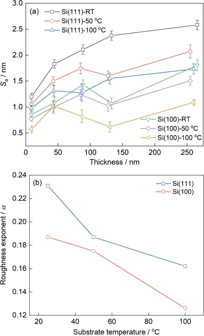
... 同时,由图7b可见,在两种取向的基底上生长的Ni5Pt合金薄膜表面粗糙度指数都随着基底温度的升高而减小.这种趋势,主要与Ni和Pt原子的迁移热能有关[22,38~40].随着基底温度的提高Ni和Pt原子的扩散能力增强,生成的薄膜表面更加均匀和起伏较小.同时,较高的基底温度有助于释放界面应力,使晶体沿能量最低方向生长并通过晶界弛豫降低应力集中造成的表面不平整[41~43].但是,过高的基底温度使溅射原子的扩散能力过强而使薄膜表面的粗糙度提高[44~46]. ...
Application and development trend of NiPt alloy sputtering target in semiconductor manufacturing
1
2016
... 基于金属-半导体结的肖特基二极管(Schottky barrier diode, SBD)的正向压降较低、超高速响应和低功耗,得到了广泛的应用[1,2].SBD的整流特性和稳定性决定于其金属-半导体势垒,常用的势垒金属有Au[3]、Pt[4]、Ni[5]和Pd[6].但是,这些传统贵金属的热稳定性较低且功函数不可调.使用合金材料替代单一贵金属可精准调控势垒高度[7,8].镍铂(NiPt)合金的热稳定性较高且界面特性可调控,是主流势垒材料[9~11].制备NiPt基SBD用的是在Si基底磁控溅射的合金薄膜,将其热处理形成热稳定的NiPtSi势垒层可实现反向电流阻断[12].关于NiPt合金的研究,侧重于NiPt薄膜与Si形成的势垒高度[13]、热稳定性[11]以及高速退火工艺等方面[14].制备NiPt合金薄膜的工艺参数对SBD器件势垒层微结构和性能的影响尚须进一步深入研究[15~17].近年来,研究人员通过调控磁控溅射制备参数(如沉积时间、基底温度和沉积速率等)改善NiPt合金薄膜的表面粗糙度并调控残余应力[9,18,19].Shin等[18]用晶圆曲率法研究了xNi(1-x)Pt (0.02 < x < 0.81)薄膜的应力行为,发现富集Ni的样品对基底温度和沉积速率的变化极其敏感.随着基底温度的降低和沉积速率的提高,薄膜中的残余应力显著增大.Eiler等[19]分析了xNi(1-x)Pt (0.01 < x < 0.39)薄膜的杨氏模量和硬度的变化,发现随着沉积时间的延长表面粗糙度有所提高.Yang等[20]发现,基底取向对ZnO薄膜的表面粗糙度也有显著影响.取向不同的基底其原子排列不同,使在其上制备的薄膜原子的生长能力也不同.在Si(100)基底上制备的薄膜表面粗糙度略比Si(111)基底的低.Tsamouras和Galinski等[21,22]发现,随着基底温度的提高在其上制备的Pt薄膜表面粗糙度提高,因为基底原子的扩散增强和活化能增大.虽然有些工作研究了用不同工艺制备的NiPt合金薄膜的表面粗糙度和残余应力状态的变化,但是关于制备工艺参数不同的Ni5Pt合金薄膜的应力变化和薄膜表面质量仍缺少系统的研究[10,16,23],特别是亟需进一步揭示薄膜制备工艺参数对薄膜的残余应力和表面粗糙度的影响.鉴于此,本文在两种晶体取向的单晶硅基底上磁控溅射Ni5Pt合金薄膜,研究基底温度、沉积时间以及基底取向对薄膜的表面粗糙度和微观结构的影响,并根据薄膜的开裂行为以及残余应力分布建立薄膜开裂的判据. ...
镍铂合金溅射靶材在半导体制造中的应用及发展趋势
1
2016
... 基于金属-半导体结的肖特基二极管(Schottky barrier diode, SBD)的正向压降较低、超高速响应和低功耗,得到了广泛的应用[1,2].SBD的整流特性和稳定性决定于其金属-半导体势垒,常用的势垒金属有Au[3]、Pt[4]、Ni[5]和Pd[6].但是,这些传统贵金属的热稳定性较低且功函数不可调.使用合金材料替代单一贵金属可精准调控势垒高度[7,8].镍铂(NiPt)合金的热稳定性较高且界面特性可调控,是主流势垒材料[9~11].制备NiPt基SBD用的是在Si基底磁控溅射的合金薄膜,将其热处理形成热稳定的NiPtSi势垒层可实现反向电流阻断[12].关于NiPt合金的研究,侧重于NiPt薄膜与Si形成的势垒高度[13]、热稳定性[11]以及高速退火工艺等方面[14].制备NiPt合金薄膜的工艺参数对SBD器件势垒层微结构和性能的影响尚须进一步深入研究[15~17].近年来,研究人员通过调控磁控溅射制备参数(如沉积时间、基底温度和沉积速率等)改善NiPt合金薄膜的表面粗糙度并调控残余应力[9,18,19].Shin等[18]用晶圆曲率法研究了xNi(1-x)Pt (0.02 < x < 0.81)薄膜的应力行为,发现富集Ni的样品对基底温度和沉积速率的变化极其敏感.随着基底温度的降低和沉积速率的提高,薄膜中的残余应力显著增大.Eiler等[19]分析了xNi(1-x)Pt (0.01 < x < 0.39)薄膜的杨氏模量和硬度的变化,发现随着沉积时间的延长表面粗糙度有所提高.Yang等[20]发现,基底取向对ZnO薄膜的表面粗糙度也有显著影响.取向不同的基底其原子排列不同,使在其上制备的薄膜原子的生长能力也不同.在Si(100)基底上制备的薄膜表面粗糙度略比Si(111)基底的低.Tsamouras和Galinski等[21,22]发现,随着基底温度的提高在其上制备的Pt薄膜表面粗糙度提高,因为基底原子的扩散增强和活化能增大.虽然有些工作研究了用不同工艺制备的NiPt合金薄膜的表面粗糙度和残余应力状态的变化,但是关于制备工艺参数不同的Ni5Pt合金薄膜的应力变化和薄膜表面质量仍缺少系统的研究[10,16,23],特别是亟需进一步揭示薄膜制备工艺参数对薄膜的残余应力和表面粗糙度的影响.鉴于此,本文在两种晶体取向的单晶硅基底上磁控溅射Ni5Pt合金薄膜,研究基底温度、沉积时间以及基底取向对薄膜的表面粗糙度和微观结构的影响,并根据薄膜的开裂行为以及残余应力分布建立薄膜开裂的判据. ...
Film thickness effect on texture and residual stress sign transition in sputtered TiN thin films
2
2017
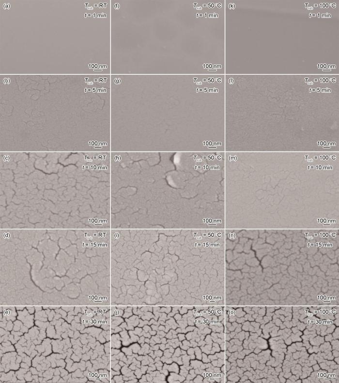
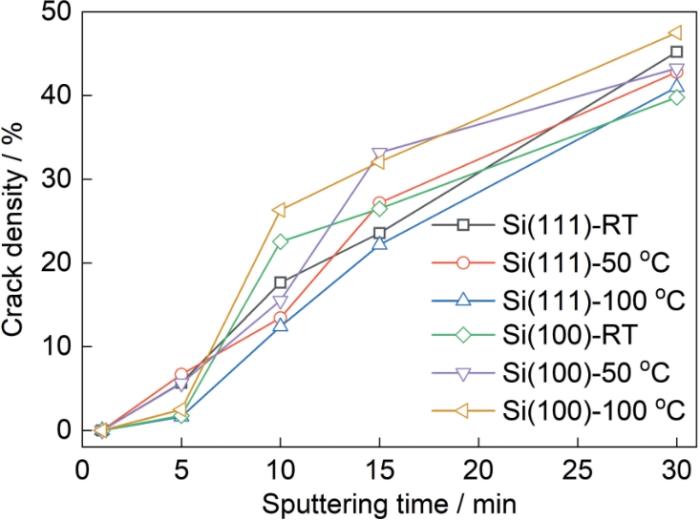
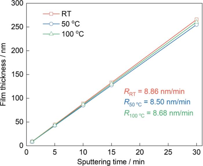
... 图1给出了分别在室温、50 ℃和100 ℃的Si(100)基底上溅射1、5、10、15和30 min制备的5种厚度的Ni5Pt薄膜样品的SEM照片.可以看出,除了沉积时间为1 min的薄膜,其余4种的表面都出现了不同程度的开裂.为了评估样品表面的开裂程度,统计了薄膜表面的裂纹密度(即SEM照片下裂纹面积占总面积的百分比),如图2所示.可以看出,随沉积时间(薄膜厚度)的增加薄膜的裂纹密度显著提高,表明裂纹的形成可能与薄膜内的应力密切相关,因为应力随着膜厚的增加而增大[24]. ...
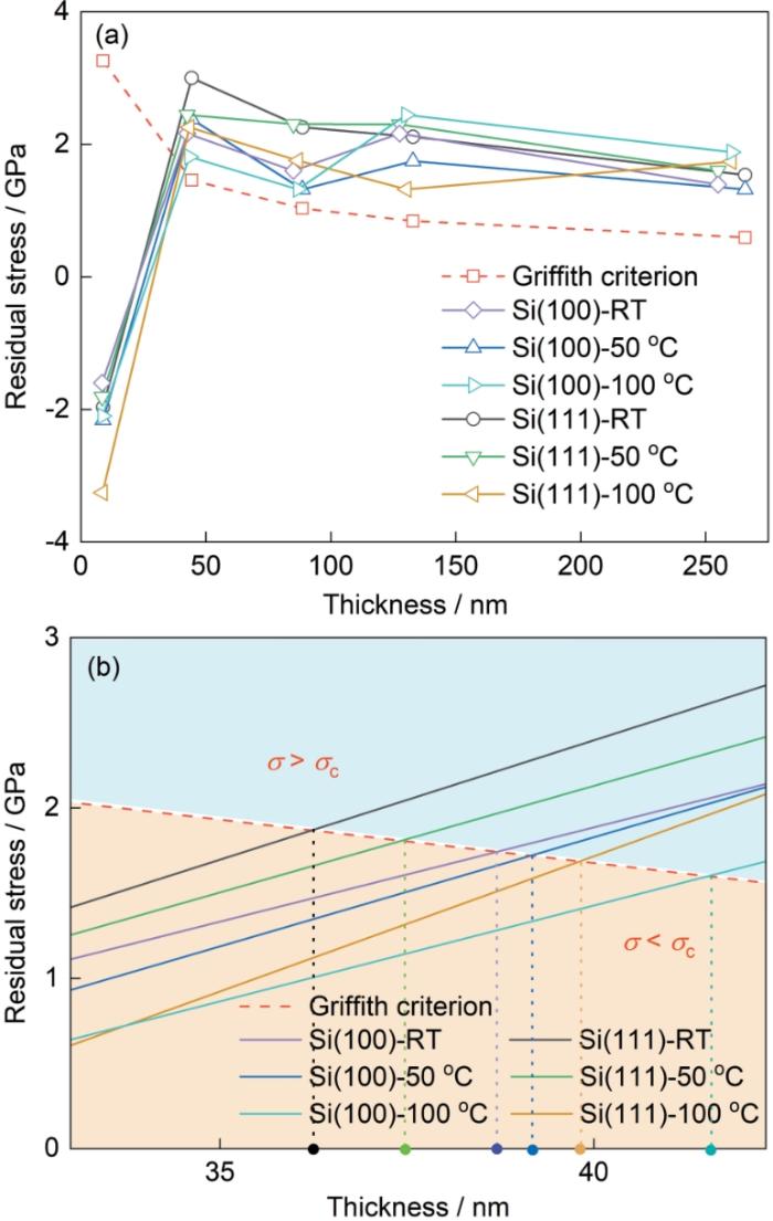
... 可计算出溅射参数不同的薄膜中的残余应力值[27],结果如图8所示. 式(4)中E和ν分别为Ni5Pt薄膜的弹性模量和泊松比,θ为布拉格衍射角,dθ 为在θ角下测得的晶面间距,d0为无应力状态晶面的晶面间距.由图8可见,随着Ni5Pt薄膜厚度的增加残余应力由压应力转变为拉应力.这一转变,可能与薄膜生长过程中内部积累的生长应力、界面失配应力和热应力有关[47~49].首先,Ni5Pt薄膜与Si基底的晶格常数和表面能不同,且Ni5Pt合金的(111)和(200)晶面间距也不同,分别为dNi5Pt(111) = 0.21 nm, dNi5Pt(200) = 0.18 nm,Si基底的(100)和(111)晶面间距分别为dSi(100) = 0.5431 nm和dSi(111) = 0.3135 nm[50];两种材料的表面能也不同,分别为γNi5Pt(111) = 2.165 J/m2 [30],γSi(100) ≈ γSi(111) = 1.23 J/m2 [31].在磁控溅射过程中,薄膜与基底的界面晶格失配,在界面产生了失配应力[48].但是,Yang等[51]和Wang等[52]认为,厚度在亚微米范围内的薄膜,其界面失配应力与总残余应力相比并不起关键作用.其次,Ni5Pt薄膜与单晶Si基底的热膨胀系数不同也在沉积和冷却过程中产生热应力[49].计算结果表明,Ni5Pt薄膜中的热应力只有0.07~0.22 GPa,占总残余应力的2.2%~6.3%,可以忽略不计.这表明,引起Ni5Pt薄膜开裂的是薄膜生长过程中微观结构变化产生的薄膜生长应力.在Ni5Pt薄膜生长的初期,“原子喷丸”效应是引起薄膜残余应力的主要机制[53].在溅射沉积过程中,入射Ar⁺的轰击使部分原子偏离晶位而产生残余压应力[52].随着沉积时间的延长表面原子的扩散不足而产生亚稳态结构,在沉积后的有序化过程填补缺陷、体积收缩使其转变为残余拉应力.当拉应力超过“原子喷丸”效应产生的压应力时,薄膜呈拉应力状态[24]. ...
Magnetism and spatial order in Ni-Pt and Co-Pt alloys
2
1986
... 图3给出了磁控溅射参数不同的Ni5Pt合金薄膜的XRD谱,可见所有样品的谱中都出现了与(111)和(200)晶面对应的衍射峰,其中较为显著的(111)峰表明薄膜中的晶粒具有一定的择优取向.随着薄膜沉积时间的延长衍射峰强度逐渐提高,表明薄膜的结晶度提高,且晶体的择优取向更加明显,生长织构逐渐增强.需要指出的是,Ni-Pt合金体系中可能存在多种中间相(如NiPt、Ni3Pt、NiPt3等[25]),且这些相的衍射峰位与Ni5Pt相的(111)和(200)面峰位较为接近.为了准确判断薄膜的相结构,将样品的XRD谱与文献中的Ni5Pt薄膜的衍射谱比较.根据Ni-Pt二元合金的平衡相图[25],在Pt含量低于约20% (原子分数)的Ni富集区间体系处于稳定的面心立方(FCC)置换固溶体区域,不生成有序金属间化合物或第二相,据此判定薄膜中出现的衍射峰对应Ni5Pt相[9,16,19].此外,所有Ni5Pt薄膜的衍射峰均向低角度偏移,表明晶格常数有所增大,其原因可能是原子半径较大的Pt原子(0.139 nm)部分取代Ni原子(0.125 nm)进入晶格位置形成了置换型固溶体,使晶胞体积膨胀[14].这种在取向和温度不同的基底制备的薄膜相同的衍射峰偏移,进一步证实了成分主导的晶格膨胀机制[26].衍射峰展宽的原因有:在低温沉积薄膜中晶粒较小和在制备过程中薄膜出现一定程度的晶格畸变或微应变,特别是Pt原子非均匀分布或局部固溶在晶格内产生了弹性畸变场[27]. ...
... [25],在Pt含量低于约20% (原子分数)的Ni富集区间体系处于稳定的面心立方(FCC)置换固溶体区域,不生成有序金属间化合物或第二相,据此判定薄膜中出现的衍射峰对应Ni5Pt相[9,16,19].此外,所有Ni5Pt薄膜的衍射峰均向低角度偏移,表明晶格常数有所增大,其原因可能是原子半径较大的Pt原子(0.139 nm)部分取代Ni原子(0.125 nm)进入晶格位置形成了置换型固溶体,使晶胞体积膨胀[14].这种在取向和温度不同的基底制备的薄膜相同的衍射峰偏移,进一步证实了成分主导的晶格膨胀机制[26].衍射峰展宽的原因有:在低温沉积薄膜中晶粒较小和在制备过程中薄膜出现一定程度的晶格畸变或微应变,特别是Pt原子非均匀分布或局部固溶在晶格内产生了弹性畸变场[27]. ...
Ni1- x Pt x (x = 0-0.12) hollow spheres as catalysts for hydrogen generation from ammonia borane
1
2007
... 图3给出了磁控溅射参数不同的Ni5Pt合金薄膜的XRD谱,可见所有样品的谱中都出现了与(111)和(200)晶面对应的衍射峰,其中较为显著的(111)峰表明薄膜中的晶粒具有一定的择优取向.随着薄膜沉积时间的延长衍射峰强度逐渐提高,表明薄膜的结晶度提高,且晶体的择优取向更加明显,生长织构逐渐增强.需要指出的是,Ni-Pt合金体系中可能存在多种中间相(如NiPt、Ni3Pt、NiPt3等[25]),且这些相的衍射峰位与Ni5Pt相的(111)和(200)面峰位较为接近.为了准确判断薄膜的相结构,将样品的XRD谱与文献中的Ni5Pt薄膜的衍射谱比较.根据Ni-Pt二元合金的平衡相图[25],在Pt含量低于约20% (原子分数)的Ni富集区间体系处于稳定的面心立方(FCC)置换固溶体区域,不生成有序金属间化合物或第二相,据此判定薄膜中出现的衍射峰对应Ni5Pt相[9,16,19].此外,所有Ni5Pt薄膜的衍射峰均向低角度偏移,表明晶格常数有所增大,其原因可能是原子半径较大的Pt原子(0.139 nm)部分取代Ni原子(0.125 nm)进入晶格位置形成了置换型固溶体,使晶胞体积膨胀[14].这种在取向和温度不同的基底制备的薄膜相同的衍射峰偏移,进一步证实了成分主导的晶格膨胀机制[26].衍射峰展宽的原因有:在低温沉积薄膜中晶粒较小和在制备过程中薄膜出现一定程度的晶格畸变或微应变,特别是Pt原子非均匀分布或局部固溶在晶格内产生了弹性畸变场[27]. ...
Stress analysis of polycrystalline thin films and surface regions by X-ray diffraction
2
2005
... 图3给出了磁控溅射参数不同的Ni5Pt合金薄膜的XRD谱,可见所有样品的谱中都出现了与(111)和(200)晶面对应的衍射峰,其中较为显著的(111)峰表明薄膜中的晶粒具有一定的择优取向.随着薄膜沉积时间的延长衍射峰强度逐渐提高,表明薄膜的结晶度提高,且晶体的择优取向更加明显,生长织构逐渐增强.需要指出的是,Ni-Pt合金体系中可能存在多种中间相(如NiPt、Ni3Pt、NiPt3等[25]),且这些相的衍射峰位与Ni5Pt相的(111)和(200)面峰位较为接近.为了准确判断薄膜的相结构,将样品的XRD谱与文献中的Ni5Pt薄膜的衍射谱比较.根据Ni-Pt二元合金的平衡相图[25],在Pt含量低于约20% (原子分数)的Ni富集区间体系处于稳定的面心立方(FCC)置换固溶体区域,不生成有序金属间化合物或第二相,据此判定薄膜中出现的衍射峰对应Ni5Pt相[9,16,19].此外,所有Ni5Pt薄膜的衍射峰均向低角度偏移,表明晶格常数有所增大,其原因可能是原子半径较大的Pt原子(0.139 nm)部分取代Ni原子(0.125 nm)进入晶格位置形成了置换型固溶体,使晶胞体积膨胀[14].这种在取向和温度不同的基底制备的薄膜相同的衍射峰偏移,进一步证实了成分主导的晶格膨胀机制[26].衍射峰展宽的原因有:在低温沉积薄膜中晶粒较小和在制备过程中薄膜出现一定程度的晶格畸变或微应变,特别是Pt原子非均匀分布或局部固溶在晶格内产生了弹性畸变场[27]. ...
... 可计算出溅射参数不同的薄膜中的残余应力值[27],结果如图8所示. 式(4)中E和ν分别为Ni5Pt薄膜的弹性模量和泊松比,θ为布拉格衍射角,dθ 为在θ角下测得的晶面间距,d0为无应力状态晶面的晶面间距.由图8可见,随着Ni5Pt薄膜厚度的增加残余应力由压应力转变为拉应力.这一转变,可能与薄膜生长过程中内部积累的生长应力、界面失配应力和热应力有关[47~49].首先,Ni5Pt薄膜与Si基底的晶格常数和表面能不同,且Ni5Pt合金的(111)和(200)晶面间距也不同,分别为dNi5Pt(111) = 0.21 nm, dNi5Pt(200) = 0.18 nm,Si基底的(100)和(111)晶面间距分别为dSi(100) = 0.5431 nm和dSi(111) = 0.3135 nm[50];两种材料的表面能也不同,分别为γNi5Pt(111) = 2.165 J/m2 [30],γSi(100) ≈ γSi(111) = 1.23 J/m2 [31].在磁控溅射过程中,薄膜与基底的界面晶格失配,在界面产生了失配应力[48].但是,Yang等[51]和Wang等[52]认为,厚度在亚微米范围内的薄膜,其界面失配应力与总残余应力相比并不起关键作用.其次,Ni5Pt薄膜与单晶Si基底的热膨胀系数不同也在沉积和冷却过程中产生热应力[49].计算结果表明,Ni5Pt薄膜中的热应力只有0.07~0.22 GPa,占总残余应力的2.2%~6.3%,可以忽略不计.这表明,引起Ni5Pt薄膜开裂的是薄膜生长过程中微观结构变化产生的薄膜生长应力.在Ni5Pt薄膜生长的初期,“原子喷丸”效应是引起薄膜残余应力的主要机制[53].在溅射沉积过程中,入射Ar⁺的轰击使部分原子偏离晶位而产生残余压应力[52].随着沉积时间的延长表面原子的扩散不足而产生亚稳态结构,在沉积后的有序化过程填补缺陷、体积收缩使其转变为残余拉应力.当拉应力超过“原子喷丸”效应产生的压应力时,薄膜呈拉应力状态[24]. ...
Effect of low surface energy material deposition on the wettability and corrosion resistance characteristics of a copper substrate
1
2025
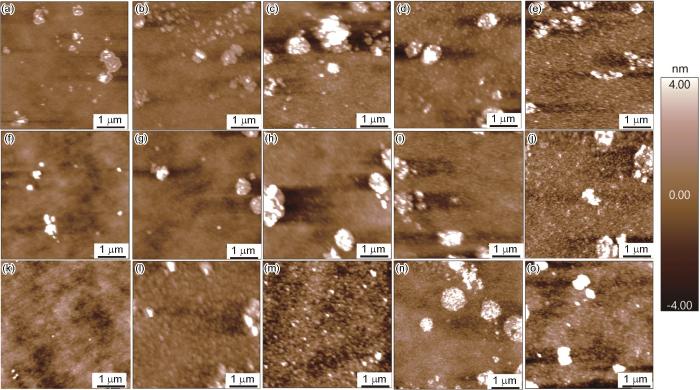
... 图5给出了Si(100)基底上不同溅射参数的Ni5Pt合金薄膜的AFM照片,可见所有样品的表面均由不同尺寸的白色团簇状颗粒构成,且颗粒的尺寸和密度随着沉积时间的增加而显著增大和提高.假设薄膜原子在基底上生成一球冠状晶核,根据界面张力的平衡关系[28] ...
First-principle study of interfacial properties of Ni-Ni3Si composite
1
2013
... 金属Ni、Pt的(111)晶面以及基底Si在(111)和(100)面的表面能分别为γNi(111) = 2.20 J/m2,γPt(111) = 1.50 J/m2,γSi(100) ≈ γSi(111) = 1.23 J/m2 [29~31]. 式 (1)中γf,γs分别为薄膜材料原子和基底材料的表面能,γi为薄膜原子与基底材料之间的界面能,θ为接触角.根据混合法则[32]可计算出Ni5Pt合金在(111)晶面的表面能为γNi5Pt(111) = 2.165 J/m2,且Ni与Si之间的界面能γi ≈ 1.80 J/m2 [33].于是可得Ni5Pt薄膜与Si基底的(111)晶面的表面能之差以及表面能之和分别为 ...
Critical assessment of Pt surface energy-An atomistic study
1
2018
... 可计算出溅射参数不同的薄膜中的残余应力值[27],结果如图8所示. 式(4)中E和ν分别为Ni5Pt薄膜的弹性模量和泊松比,θ为布拉格衍射角,dθ 为在θ角下测得的晶面间距,d0为无应力状态晶面的晶面间距.由图8可见,随着Ni5Pt薄膜厚度的增加残余应力由压应力转变为拉应力.这一转变,可能与薄膜生长过程中内部积累的生长应力、界面失配应力和热应力有关[47~49].首先,Ni5Pt薄膜与Si基底的晶格常数和表面能不同,且Ni5Pt合金的(111)和(200)晶面间距也不同,分别为dNi5Pt(111) = 0.21 nm, dNi5Pt(200) = 0.18 nm,Si基底的(100)和(111)晶面间距分别为dSi(100) = 0.5431 nm和dSi(111) = 0.3135 nm[50];两种材料的表面能也不同,分别为γNi5Pt(111) = 2.165 J/m2 [30],γSi(100) ≈ γSi(111) = 1.23 J/m2 [31].在磁控溅射过程中,薄膜与基底的界面晶格失配,在界面产生了失配应力[48].但是,Yang等[51]和Wang等[52]认为,厚度在亚微米范围内的薄膜,其界面失配应力与总残余应力相比并不起关键作用.其次,Ni5Pt薄膜与单晶Si基底的热膨胀系数不同也在沉积和冷却过程中产生热应力[49].计算结果表明,Ni5Pt薄膜中的热应力只有0.07~0.22 GPa,占总残余应力的2.2%~6.3%,可以忽略不计.这表明,引起Ni5Pt薄膜开裂的是薄膜生长过程中微观结构变化产生的薄膜生长应力.在Ni5Pt薄膜生长的初期,“原子喷丸”效应是引起薄膜残余应力的主要机制[53].在溅射沉积过程中,入射Ar⁺的轰击使部分原子偏离晶位而产生残余压应力[52].随着沉积时间的延长表面原子的扩散不足而产生亚稳态结构,在沉积后的有序化过程填补缺陷、体积收缩使其转变为残余拉应力.当拉应力超过“原子喷丸”效应产生的压应力时,薄膜呈拉应力状态[24]. ...
Surface energy of germanium and silicon
3
1963
... 金属Ni、Pt的(111)晶面以及基底Si在(111)和(100)面的表面能分别为γNi(111) = 2.20 J/m2,γPt(111) = 1.50 J/m2,γSi(100) ≈ γSi(111) = 1.23 J/m2 [29~31]. 式 (1)中γf,γs分别为薄膜材料原子和基底材料的表面能,γi为薄膜原子与基底材料之间的界面能,θ为接触角.根据混合法则[32]可计算出Ni5Pt合金在(111)晶面的表面能为γNi5Pt(111) = 2.165 J/m2,且Ni与Si之间的界面能γi ≈ 1.80 J/m2 [33].于是可得Ni5Pt薄膜与Si基底的(111)晶面的表面能之差以及表面能之和分别为 ...
... 式(3)表明,ln(Sa)-ln(h)呈线性关系,进行线性拟合可得磁控溅射参数不同的Ni5Pt薄膜的α值.图7b给出了Ni5Pt薄膜的α与基底温度的关系.可以看出,与在Si(100)基底制备的薄膜相比,在Si(111)基底上制备的Ni5Pt薄膜其α更大.这一差异,与两种取向基底的原子排列方式以及Ni和Pt原子在Si基底表面的扩散特性密切相关.虽然Si(100)基底与Si(111)基底的表面能接近(γSi(100) ≈ γSi(111) = 1.23 J/m2)[31],且Ni和Pt原子在两种取向基底表面上的扩散能力接近,但是Si(111)基底原子的排列更紧密,原子扩散激活能较高((0.97 ± 0.07) eV)[36],溅射出的Ni和Pt原子局部聚集形成较大的颗粒或岛状结构,使薄膜的表面粗糙度提高.而Si(100)基底表面的低能台阶和活性位点较多,原子激活能较低(~0.60 eV)[37],Ni和Pt原子更容易沿着台阶移动填充空位而生成表面较为平整的薄膜. ...
... 可计算出溅射参数不同的薄膜中的残余应力值[27],结果如图8所示. 式(4)中E和ν分别为Ni5Pt薄膜的弹性模量和泊松比,θ为布拉格衍射角,dθ 为在θ角下测得的晶面间距,d0为无应力状态晶面的晶面间距.由图8可见,随着Ni5Pt薄膜厚度的增加残余应力由压应力转变为拉应力.这一转变,可能与薄膜生长过程中内部积累的生长应力、界面失配应力和热应力有关[47~49].首先,Ni5Pt薄膜与Si基底的晶格常数和表面能不同,且Ni5Pt合金的(111)和(200)晶面间距也不同,分别为dNi5Pt(111) = 0.21 nm, dNi5Pt(200) = 0.18 nm,Si基底的(100)和(111)晶面间距分别为dSi(100) = 0.5431 nm和dSi(111) = 0.3135 nm[50];两种材料的表面能也不同,分别为γNi5Pt(111) = 2.165 J/m2 [30],γSi(100) ≈ γSi(111) = 1.23 J/m2 [31].在磁控溅射过程中,薄膜与基底的界面晶格失配,在界面产生了失配应力[48].但是,Yang等[51]和Wang等[52]认为,厚度在亚微米范围内的薄膜,其界面失配应力与总残余应力相比并不起关键作用.其次,Ni5Pt薄膜与单晶Si基底的热膨胀系数不同也在沉积和冷却过程中产生热应力[49].计算结果表明,Ni5Pt薄膜中的热应力只有0.07~0.22 GPa,占总残余应力的2.2%~6.3%,可以忽略不计.这表明,引起Ni5Pt薄膜开裂的是薄膜生长过程中微观结构变化产生的薄膜生长应力.在Ni5Pt薄膜生长的初期,“原子喷丸”效应是引起薄膜残余应力的主要机制[53].在溅射沉积过程中,入射Ar⁺的轰击使部分原子偏离晶位而产生残余压应力[52].随着沉积时间的延长表面原子的扩散不足而产生亚稳态结构,在沉积后的有序化过程填补缺陷、体积收缩使其转变为残余拉应力.当拉应力超过“原子喷丸”效应产生的压应力时,薄膜呈拉应力状态[24]. ...
Deformation of sandwich sheet materials in uniaxial tension
1
1979
... 金属Ni、Pt的(111)晶面以及基底Si在(111)和(100)面的表面能分别为γNi(111) = 2.20 J/m2,γPt(111) = 1.50 J/m2,γSi(100) ≈ γSi(111) = 1.23 J/m2 [29~31]. 式 (1)中γf,γs分别为薄膜材料原子和基底材料的表面能,γi为薄膜原子与基底材料之间的界面能,θ为接触角.根据混合法则[32]可计算出Ni5Pt合金在(111)晶面的表面能为γNi5Pt(111) = 2.165 J/m2,且Ni与Si之间的界面能γi ≈ 1.80 J/m2 [33].于是可得Ni5Pt薄膜与Si基底的(111)晶面的表面能之差以及表面能之和分别为 ...
Density functional theory study of the interfacial properties of Ni/Ni3Si eutectic alloy
1
2014
... 金属Ni、Pt的(111)晶面以及基底Si在(111)和(100)面的表面能分别为γNi(111) = 2.20 J/m2,γPt(111) = 1.50 J/m2,γSi(100) ≈ γSi(111) = 1.23 J/m2 [29~31]. 式 (1)中γf,γs分别为薄膜材料原子和基底材料的表面能,γi为薄膜原子与基底材料之间的界面能,θ为接触角.根据混合法则[32]可计算出Ni5Pt合金在(111)晶面的表面能为γNi5Pt(111) = 2.165 J/m2,且Ni与Si之间的界面能γi ≈ 1.80 J/m2 [33].于是可得Ni5Pt薄膜与Si基底的(111)晶面的表面能之差以及表面能之和分别为 ...
Nucleation and growth of thin films
1
1984
... γNi5Pt(111) - γSi(111) = 0.935 J/m2,γNi5Pt(111) + γSi(111) = 3.395 J/m2,可见满足γNi5Pt - γSi < γi < γNi5Pt + γSi (0.935 J/m2 < 1.80 J/m2 < 3.395 J/m2)条件[34].这表明,Ni5Pt薄膜在Si基底上的生长模式符合典型的层-岛状(Stranski-Krastanov, SK)生长模式. ...
Scaling of the active zone in the Eden process on percolation networks and the ballistic deposition model
1
1985
... 制备参数不同的Ni5Pt合金薄膜样品的表面粗糙度,如图7所示.可见,在Si(111)基底上制备的Ni5Pt薄膜其表面粗糙度均高于在Si(100)基底制备的薄膜样品.图7a给出了Ni5Pt薄膜的表面粗糙度与制备参数的关系:随着沉积时间(薄膜厚度)的增加,表面粗糙度随之提高.可用动力学标度理论[35]描述Ni5Pt薄膜的表面粗糙度(Sa)与薄膜厚度(h)的关系 ...
Calculated Schwoebel barriers on Si(111) steps using an empirical potential
1
1996
... 式(3)表明,ln(Sa)-ln(h)呈线性关系,进行线性拟合可得磁控溅射参数不同的Ni5Pt薄膜的α值.图7b给出了Ni5Pt薄膜的α与基底温度的关系.可以看出,与在Si(100)基底制备的薄膜相比,在Si(111)基底上制备的Ni5Pt薄膜其α更大.这一差异,与两种取向基底的原子排列方式以及Ni和Pt原子在Si基底表面的扩散特性密切相关.虽然Si(100)基底与Si(111)基底的表面能接近(γSi(100) ≈ γSi(111) = 1.23 J/m2)[31],且Ni和Pt原子在两种取向基底表面上的扩散能力接近,但是Si(111)基底原子的排列更紧密,原子扩散激活能较高((0.97 ± 0.07) eV)[36],溅射出的Ni和Pt原子局部聚集形成较大的颗粒或岛状结构,使薄膜的表面粗糙度提高.而Si(100)基底表面的低能台阶和活性位点较多,原子激活能较低(~0.60 eV)[37],Ni和Pt原子更容易沿着台阶移动填充空位而生成表面较为平整的薄膜. ...
Binding and diffusion of a Si adatom on the Si(100) surface
1
1991
... 式(3)表明,ln(Sa)-ln(h)呈线性关系,进行线性拟合可得磁控溅射参数不同的Ni5Pt薄膜的α值.图7b给出了Ni5Pt薄膜的α与基底温度的关系.可以看出,与在Si(100)基底制备的薄膜相比,在Si(111)基底上制备的Ni5Pt薄膜其α更大.这一差异,与两种取向基底的原子排列方式以及Ni和Pt原子在Si基底表面的扩散特性密切相关.虽然Si(100)基底与Si(111)基底的表面能接近(γSi(100) ≈ γSi(111) = 1.23 J/m2)[31],且Ni和Pt原子在两种取向基底表面上的扩散能力接近,但是Si(111)基底原子的排列更紧密,原子扩散激活能较高((0.97 ± 0.07) eV)[36],溅射出的Ni和Pt原子局部聚集形成较大的颗粒或岛状结构,使薄膜的表面粗糙度提高.而Si(100)基底表面的低能台阶和活性位点较多,原子激活能较低(~0.60 eV)[37],Ni和Pt原子更容易沿着台阶移动填充空位而生成表面较为平整的薄膜. ...
Molecular dynamics simulation of nanoscale surface diffusion of heterogeneous adatoms clusters
1
2016
... 同时,由图7b可见,在两种取向的基底上生长的Ni5Pt合金薄膜表面粗糙度指数都随着基底温度的升高而减小.这种趋势,主要与Ni和Pt原子的迁移热能有关[22,38~40].随着基底温度的提高Ni和Pt原子的扩散能力增强,生成的薄膜表面更加均匀和起伏较小.同时,较高的基底温度有助于释放界面应力,使晶体沿能量最低方向生长并通过晶界弛豫降低应力集中造成的表面不平整[41~43].但是,过高的基底温度使溅射原子的扩散能力过强而使薄膜表面的粗糙度提高[44~46]. ...
Diffusion and magnetization of metal adatoms on single-layer molybdenum disulfide at elevated temperatures
0
2024
Epitaxial growth of silver on mica as studied by AFM and STM
1
1994
... 同时,由图7b可见,在两种取向的基底上生长的Ni5Pt合金薄膜表面粗糙度指数都随着基底温度的升高而减小.这种趋势,主要与Ni和Pt原子的迁移热能有关[22,38~40].随着基底温度的提高Ni和Pt原子的扩散能力增强,生成的薄膜表面更加均匀和起伏较小.同时,较高的基底温度有助于释放界面应力,使晶体沿能量最低方向生长并通过晶界弛豫降低应力集中造成的表面不平整[41~43].但是,过高的基底温度使溅射原子的扩散能力过强而使薄膜表面的粗糙度提高[44~46]. ...
Growth temperature and relaxation of lattice strain in epitaxial Pt films exhibiting diffraction fringes
1
2019
... 同时,由图7b可见,在两种取向的基底上生长的Ni5Pt合金薄膜表面粗糙度指数都随着基底温度的升高而减小.这种趋势,主要与Ni和Pt原子的迁移热能有关[22,38~40].随着基底温度的提高Ni和Pt原子的扩散能力增强,生成的薄膜表面更加均匀和起伏较小.同时,较高的基底温度有助于释放界面应力,使晶体沿能量最低方向生长并通过晶界弛豫降低应力集中造成的表面不平整[41~43].但是,过高的基底温度使溅射原子的扩散能力过强而使薄膜表面的粗糙度提高[44~46]. ...
Stress origin and relaxation in epitaxial AIN thin films on SiC
0
2001
Effects of strain on ultrahigh-performance optoelectronics and growth behavior of high-quality indium tin oxide films on yttria-stabilized zirconia (001) substrates
1
2021
... 同时,由图7b可见,在两种取向的基底上生长的Ni5Pt合金薄膜表面粗糙度指数都随着基底温度的升高而减小.这种趋势,主要与Ni和Pt原子的迁移热能有关[22,38~40].随着基底温度的提高Ni和Pt原子的扩散能力增强,生成的薄膜表面更加均匀和起伏较小.同时,较高的基底温度有助于释放界面应力,使晶体沿能量最低方向生长并通过晶界弛豫降低应力集中造成的表面不平整[41~43].但是,过高的基底温度使溅射原子的扩散能力过强而使薄膜表面的粗糙度提高[44~46]. ...
Effect of substrate temperature on variations in the structural and optical properties of Cu2O thin films deposited via RF magnetron sputtering
1
2023
... 同时,由图7b可见,在两种取向的基底上生长的Ni5Pt合金薄膜表面粗糙度指数都随着基底温度的升高而减小.这种趋势,主要与Ni和Pt原子的迁移热能有关[22,38~40].随着基底温度的提高Ni和Pt原子的扩散能力增强,生成的薄膜表面更加均匀和起伏较小.同时,较高的基底温度有助于释放界面应力,使晶体沿能量最低方向生长并通过晶界弛豫降低应力集中造成的表面不平整[41~43].但是,过高的基底温度使溅射原子的扩散能力过强而使薄膜表面的粗糙度提高[44~46]. ...
Effect of silicon substrate temperature on properties of Ti films prepared by electron beam evaporation
0
2024
硅衬底温度对电子束蒸发钛薄膜性能的影响
0
2024
Influence of substrate temperature on growth of RF sputtered bismuth telluride films
1
2012
... 同时,由图7b可见,在两种取向的基底上生长的Ni5Pt合金薄膜表面粗糙度指数都随着基底温度的升高而减小.这种趋势,主要与Ni和Pt原子的迁移热能有关[22,38~40].随着基底温度的提高Ni和Pt原子的扩散能力增强,生成的薄膜表面更加均匀和起伏较小.同时,较高的基底温度有助于释放界面应力,使晶体沿能量最低方向生长并通过晶界弛豫降低应力集中造成的表面不平整[41~43].但是,过高的基底温度使溅射原子的扩散能力过强而使薄膜表面的粗糙度提高[44~46]. ...
基片温度对射频磁控溅射碲化铋薄膜微结构和表面形貌的影响
1
2012
... 同时,由图7b可见,在两种取向的基底上生长的Ni5Pt合金薄膜表面粗糙度指数都随着基底温度的升高而减小.这种趋势,主要与Ni和Pt原子的迁移热能有关[22,38~40].随着基底温度的提高Ni和Pt原子的扩散能力增强,生成的薄膜表面更加均匀和起伏较小.同时,较高的基底温度有助于释放界面应力,使晶体沿能量最低方向生长并通过晶界弛豫降低应力集中造成的表面不平整[41~43].但是,过高的基底温度使溅射原子的扩散能力过强而使薄膜表面的粗糙度提高[44~46]. ...
The intrinsic stress of polycrystalline and epitaxial thin metal films
1
1994
... 可计算出溅射参数不同的薄膜中的残余应力值[27],结果如图8所示. 式(4)中E和ν分别为Ni5Pt薄膜的弹性模量和泊松比,θ为布拉格衍射角,dθ 为在θ角下测得的晶面间距,d0为无应力状态晶面的晶面间距.由图8可见,随着Ni5Pt薄膜厚度的增加残余应力由压应力转变为拉应力.这一转变,可能与薄膜生长过程中内部积累的生长应力、界面失配应力和热应力有关[47~49].首先,Ni5Pt薄膜与Si基底的晶格常数和表面能不同,且Ni5Pt合金的(111)和(200)晶面间距也不同,分别为dNi5Pt(111) = 0.21 nm, dNi5Pt(200) = 0.18 nm,Si基底的(100)和(111)晶面间距分别为dSi(100) = 0.5431 nm和dSi(111) = 0.3135 nm[50];两种材料的表面能也不同,分别为γNi5Pt(111) = 2.165 J/m2 [30],γSi(100) ≈ γSi(111) = 1.23 J/m2 [31].在磁控溅射过程中,薄膜与基底的界面晶格失配,在界面产生了失配应力[48].但是,Yang等[51]和Wang等[52]认为,厚度在亚微米范围内的薄膜,其界面失配应力与总残余应力相比并不起关键作用.其次,Ni5Pt薄膜与单晶Si基底的热膨胀系数不同也在沉积和冷却过程中产生热应力[49].计算结果表明,Ni5Pt薄膜中的热应力只有0.07~0.22 GPa,占总残余应力的2.2%~6.3%,可以忽略不计.这表明,引起Ni5Pt薄膜开裂的是薄膜生长过程中微观结构变化产生的薄膜生长应力.在Ni5Pt薄膜生长的初期,“原子喷丸”效应是引起薄膜残余应力的主要机制[53].在溅射沉积过程中,入射Ar⁺的轰击使部分原子偏离晶位而产生残余压应力[52].随着沉积时间的延长表面原子的扩散不足而产生亚稳态结构,在沉积后的有序化过程填补缺陷、体积收缩使其转变为残余拉应力.当拉应力超过“原子喷丸”效应产生的压应力时,薄膜呈拉应力状态[24]. ...
One-dimensional dislocations. II. Misfitting monolayers and oriented overgrowth
1
1949
... 可计算出溅射参数不同的薄膜中的残余应力值[27],结果如图8所示. 式(4)中E和ν分别为Ni5Pt薄膜的弹性模量和泊松比,θ为布拉格衍射角,dθ 为在θ角下测得的晶面间距,d0为无应力状态晶面的晶面间距.由图8可见,随着Ni5Pt薄膜厚度的增加残余应力由压应力转变为拉应力.这一转变,可能与薄膜生长过程中内部积累的生长应力、界面失配应力和热应力有关[47~49].首先,Ni5Pt薄膜与Si基底的晶格常数和表面能不同,且Ni5Pt合金的(111)和(200)晶面间距也不同,分别为dNi5Pt(111) = 0.21 nm, dNi5Pt(200) = 0.18 nm,Si基底的(100)和(111)晶面间距分别为dSi(100) = 0.5431 nm和dSi(111) = 0.3135 nm[50];两种材料的表面能也不同,分别为γNi5Pt(111) = 2.165 J/m2 [30],γSi(100) ≈ γSi(111) = 1.23 J/m2 [31].在磁控溅射过程中,薄膜与基底的界面晶格失配,在界面产生了失配应力[48].但是,Yang等[51]和Wang等[52]认为,厚度在亚微米范围内的薄膜,其界面失配应力与总残余应力相比并不起关键作用.其次,Ni5Pt薄膜与单晶Si基底的热膨胀系数不同也在沉积和冷却过程中产生热应力[49].计算结果表明,Ni5Pt薄膜中的热应力只有0.07~0.22 GPa,占总残余应力的2.2%~6.3%,可以忽略不计.这表明,引起Ni5Pt薄膜开裂的是薄膜生长过程中微观结构变化产生的薄膜生长应力.在Ni5Pt薄膜生长的初期,“原子喷丸”效应是引起薄膜残余应力的主要机制[53].在溅射沉积过程中,入射Ar⁺的轰击使部分原子偏离晶位而产生残余压应力[52].随着沉积时间的延长表面原子的扩散不足而产生亚稳态结构,在沉积后的有序化过程填补缺陷、体积收缩使其转变为残余拉应力.当拉应力超过“原子喷丸”效应产生的压应力时,薄膜呈拉应力状态[24]. ...
Mechanical integrity in PVD coatings due to the presence of residual stresses
2
2001
... 可计算出溅射参数不同的薄膜中的残余应力值[27],结果如图8所示. 式(4)中E和ν分别为Ni5Pt薄膜的弹性模量和泊松比,θ为布拉格衍射角,dθ 为在θ角下测得的晶面间距,d0为无应力状态晶面的晶面间距.由图8可见,随着Ni5Pt薄膜厚度的增加残余应力由压应力转变为拉应力.这一转变,可能与薄膜生长过程中内部积累的生长应力、界面失配应力和热应力有关[47~49].首先,Ni5Pt薄膜与Si基底的晶格常数和表面能不同,且Ni5Pt合金的(111)和(200)晶面间距也不同,分别为dNi5Pt(111) = 0.21 nm, dNi5Pt(200) = 0.18 nm,Si基底的(100)和(111)晶面间距分别为dSi(100) = 0.5431 nm和dSi(111) = 0.3135 nm[50];两种材料的表面能也不同,分别为γNi5Pt(111) = 2.165 J/m2 [30],γSi(100) ≈ γSi(111) = 1.23 J/m2 [31].在磁控溅射过程中,薄膜与基底的界面晶格失配,在界面产生了失配应力[48].但是,Yang等[51]和Wang等[52]认为,厚度在亚微米范围内的薄膜,其界面失配应力与总残余应力相比并不起关键作用.其次,Ni5Pt薄膜与单晶Si基底的热膨胀系数不同也在沉积和冷却过程中产生热应力[49].计算结果表明,Ni5Pt薄膜中的热应力只有0.07~0.22 GPa,占总残余应力的2.2%~6.3%,可以忽略不计.这表明,引起Ni5Pt薄膜开裂的是薄膜生长过程中微观结构变化产生的薄膜生长应力.在Ni5Pt薄膜生长的初期,“原子喷丸”效应是引起薄膜残余应力的主要机制[53].在溅射沉积过程中,入射Ar⁺的轰击使部分原子偏离晶位而产生残余压应力[52].随着沉积时间的延长表面原子的扩散不足而产生亚稳态结构,在沉积后的有序化过程填补缺陷、体积收缩使其转变为残余拉应力.当拉应力超过“原子喷丸”效应产生的压应力时,薄膜呈拉应力状态[24]. ...
... [49].计算结果表明,Ni5Pt薄膜中的热应力只有0.07~0.22 GPa,占总残余应力的2.2%~6.3%,可以忽略不计.这表明,引起Ni5Pt薄膜开裂的是薄膜生长过程中微观结构变化产生的薄膜生长应力.在Ni5Pt薄膜生长的初期,“原子喷丸”效应是引起薄膜残余应力的主要机制[53].在溅射沉积过程中,入射Ar⁺的轰击使部分原子偏离晶位而产生残余压应力[52].随着沉积时间的延长表面原子的扩散不足而产生亚稳态结构,在沉积后的有序化过程填补缺陷、体积收缩使其转变为残余拉应力.当拉应力超过“原子喷丸”效应产生的压应力时,薄膜呈拉应力状态[24]. ...
1
2004
... 可计算出溅射参数不同的薄膜中的残余应力值[27],结果如图8所示. 式(4)中E和ν分别为Ni5Pt薄膜的弹性模量和泊松比,θ为布拉格衍射角,dθ 为在θ角下测得的晶面间距,d0为无应力状态晶面的晶面间距.由图8可见,随着Ni5Pt薄膜厚度的增加残余应力由压应力转变为拉应力.这一转变,可能与薄膜生长过程中内部积累的生长应力、界面失配应力和热应力有关[47~49].首先,Ni5Pt薄膜与Si基底的晶格常数和表面能不同,且Ni5Pt合金的(111)和(200)晶面间距也不同,分别为dNi5Pt(111) = 0.21 nm, dNi5Pt(200) = 0.18 nm,Si基底的(100)和(111)晶面间距分别为dSi(100) = 0.5431 nm和dSi(111) = 0.3135 nm[50];两种材料的表面能也不同,分别为γNi5Pt(111) = 2.165 J/m2 [30],γSi(100) ≈ γSi(111) = 1.23 J/m2 [31].在磁控溅射过程中,薄膜与基底的界面晶格失配,在界面产生了失配应力[48].但是,Yang等[51]和Wang等[52]认为,厚度在亚微米范围内的薄膜,其界面失配应力与总残余应力相比并不起关键作用.其次,Ni5Pt薄膜与单晶Si基底的热膨胀系数不同也在沉积和冷却过程中产生热应力[49].计算结果表明,Ni5Pt薄膜中的热应力只有0.07~0.22 GPa,占总残余应力的2.2%~6.3%,可以忽略不计.这表明,引起Ni5Pt薄膜开裂的是薄膜生长过程中微观结构变化产生的薄膜生长应力.在Ni5Pt薄膜生长的初期,“原子喷丸”效应是引起薄膜残余应力的主要机制[53].在溅射沉积过程中,入射Ar⁺的轰击使部分原子偏离晶位而产生残余压应力[52].随着沉积时间的延长表面原子的扩散不足而产生亚稳态结构,在沉积后的有序化过程填补缺陷、体积收缩使其转变为残余拉应力.当拉应力超过“原子喷丸”效应产生的压应力时,薄膜呈拉应力状态[24]. ...
Metal-insulator transition characteristics of VO2 thin films grown on Ge(100) single crystals
1
2010
... 可计算出溅射参数不同的薄膜中的残余应力值[27],结果如图8所示. 式(4)中E和ν分别为Ni5Pt薄膜的弹性模量和泊松比,θ为布拉格衍射角,dθ 为在θ角下测得的晶面间距,d0为无应力状态晶面的晶面间距.由图8可见,随着Ni5Pt薄膜厚度的增加残余应力由压应力转变为拉应力.这一转变,可能与薄膜生长过程中内部积累的生长应力、界面失配应力和热应力有关[47~49].首先,Ni5Pt薄膜与Si基底的晶格常数和表面能不同,且Ni5Pt合金的(111)和(200)晶面间距也不同,分别为dNi5Pt(111) = 0.21 nm, dNi5Pt(200) = 0.18 nm,Si基底的(100)和(111)晶面间距分别为dSi(100) = 0.5431 nm和dSi(111) = 0.3135 nm[50];两种材料的表面能也不同,分别为γNi5Pt(111) = 2.165 J/m2 [30],γSi(100) ≈ γSi(111) = 1.23 J/m2 [31].在磁控溅射过程中,薄膜与基底的界面晶格失配,在界面产生了失配应力[48].但是,Yang等[51]和Wang等[52]认为,厚度在亚微米范围内的薄膜,其界面失配应力与总残余应力相比并不起关键作用.其次,Ni5Pt薄膜与单晶Si基底的热膨胀系数不同也在沉积和冷却过程中产生热应力[49].计算结果表明,Ni5Pt薄膜中的热应力只有0.07~0.22 GPa,占总残余应力的2.2%~6.3%,可以忽略不计.这表明,引起Ni5Pt薄膜开裂的是薄膜生长过程中微观结构变化产生的薄膜生长应力.在Ni5Pt薄膜生长的初期,“原子喷丸”效应是引起薄膜残余应力的主要机制[53].在溅射沉积过程中,入射Ar⁺的轰击使部分原子偏离晶位而产生残余压应力[52].随着沉积时间的延长表面原子的扩散不足而产生亚稳态结构,在沉积后的有序化过程填补缺陷、体积收缩使其转变为残余拉应力.当拉应力超过“原子喷丸”效应产生的压应力时,薄膜呈拉应力状态[24]. ...
Effects of film thickness on the residual stress of vanadium dioxide thin films grown by magnetron sputtering
2
2023
... 可计算出溅射参数不同的薄膜中的残余应力值[27],结果如图8所示. 式(4)中E和ν分别为Ni5Pt薄膜的弹性模量和泊松比,θ为布拉格衍射角,dθ 为在θ角下测得的晶面间距,d0为无应力状态晶面的晶面间距.由图8可见,随着Ni5Pt薄膜厚度的增加残余应力由压应力转变为拉应力.这一转变,可能与薄膜生长过程中内部积累的生长应力、界面失配应力和热应力有关[47~49].首先,Ni5Pt薄膜与Si基底的晶格常数和表面能不同,且Ni5Pt合金的(111)和(200)晶面间距也不同,分别为dNi5Pt(111) = 0.21 nm, dNi5Pt(200) = 0.18 nm,Si基底的(100)和(111)晶面间距分别为dSi(100) = 0.5431 nm和dSi(111) = 0.3135 nm[50];两种材料的表面能也不同,分别为γNi5Pt(111) = 2.165 J/m2 [30],γSi(100) ≈ γSi(111) = 1.23 J/m2 [31].在磁控溅射过程中,薄膜与基底的界面晶格失配,在界面产生了失配应力[48].但是,Yang等[51]和Wang等[52]认为,厚度在亚微米范围内的薄膜,其界面失配应力与总残余应力相比并不起关键作用.其次,Ni5Pt薄膜与单晶Si基底的热膨胀系数不同也在沉积和冷却过程中产生热应力[49].计算结果表明,Ni5Pt薄膜中的热应力只有0.07~0.22 GPa,占总残余应力的2.2%~6.3%,可以忽略不计.这表明,引起Ni5Pt薄膜开裂的是薄膜生长过程中微观结构变化产生的薄膜生长应力.在Ni5Pt薄膜生长的初期,“原子喷丸”效应是引起薄膜残余应力的主要机制[53].在溅射沉积过程中,入射Ar⁺的轰击使部分原子偏离晶位而产生残余压应力[52].随着沉积时间的延长表面原子的扩散不足而产生亚稳态结构,在沉积后的有序化过程填补缺陷、体积收缩使其转变为残余拉应力.当拉应力超过“原子喷丸”效应产生的压应力时,薄膜呈拉应力状态[24]. ...
... [52].随着沉积时间的延长表面原子的扩散不足而产生亚稳态结构,在沉积后的有序化过程填补缺陷、体积收缩使其转变为残余拉应力.当拉应力超过“原子喷丸”效应产生的压应力时,薄膜呈拉应力状态[24]. ...
Intrinsic stress in sputter-deposited thin films
1
1992
... 可计算出溅射参数不同的薄膜中的残余应力值[27],结果如图8所示. 式(4)中E和ν分别为Ni5Pt薄膜的弹性模量和泊松比,θ为布拉格衍射角,dθ 为在θ角下测得的晶面间距,d0为无应力状态晶面的晶面间距.由图8可见,随着Ni5Pt薄膜厚度的增加残余应力由压应力转变为拉应力.这一转变,可能与薄膜生长过程中内部积累的生长应力、界面失配应力和热应力有关[47~49].首先,Ni5Pt薄膜与Si基底的晶格常数和表面能不同,且Ni5Pt合金的(111)和(200)晶面间距也不同,分别为dNi5Pt(111) = 0.21 nm, dNi5Pt(200) = 0.18 nm,Si基底的(100)和(111)晶面间距分别为dSi(100) = 0.5431 nm和dSi(111) = 0.3135 nm[50];两种材料的表面能也不同,分别为γNi5Pt(111) = 2.165 J/m2 [30],γSi(100) ≈ γSi(111) = 1.23 J/m2 [31].在磁控溅射过程中,薄膜与基底的界面晶格失配,在界面产生了失配应力[48].但是,Yang等[51]和Wang等[52]认为,厚度在亚微米范围内的薄膜,其界面失配应力与总残余应力相比并不起关键作用.其次,Ni5Pt薄膜与单晶Si基底的热膨胀系数不同也在沉积和冷却过程中产生热应力[49].计算结果表明,Ni5Pt薄膜中的热应力只有0.07~0.22 GPa,占总残余应力的2.2%~6.3%,可以忽略不计.这表明,引起Ni5Pt薄膜开裂的是薄膜生长过程中微观结构变化产生的薄膜生长应力.在Ni5Pt薄膜生长的初期,“原子喷丸”效应是引起薄膜残余应力的主要机制[53].在溅射沉积过程中,入射Ar⁺的轰击使部分原子偏离晶位而产生残余压应力[52].随着沉积时间的延长表面原子的扩散不足而产生亚稳态结构,在沉积后的有序化过程填补缺陷、体积收缩使其转变为残余拉应力.当拉应力超过“原子喷丸”效应产生的压应力时,薄膜呈拉应力状态[24]. ...
A review on phase-field models of brittle fracture and a new fast hybrid formulation
1
2015
... 为了找出薄膜的开裂条件,假设薄膜表面的裂纹为贯穿裂纹,即裂纹的长度是薄膜的厚度,则可将薄膜开裂近似为脆性断裂.根据Griffith准则[54],薄膜材料发生断裂所需的临界应力为 ...
Epitaxial growth of nickel on Si(100) by DC magnetron sputtering
1
2008
... 式中Ef为薄膜的弹性模量,γf为薄膜的表面能,a为裂纹的半长度.由 式(5)可计算出不同厚度Ni5Pt薄膜的临界断裂应力(即断裂强度,图8a).根据图8a和XRD谱计算出残余应力,可建立薄膜发生失效断裂的判据:薄膜的残余应力小于其断裂强度即σ ≤ σc时,薄膜不会发生开裂;当σ > σc时,薄膜表面发生失效开裂.图8b给出了较薄Ni5Pt薄膜的残余应力与其断裂强度交汇区域数据.表2进一步汇总了不同制备参数下Ni5Pt薄膜发生断裂时对应的临界厚度和临界沉积时间.结果表明,在基底温度相同的条件下,在Si(100)基底上制备的薄膜发生开裂的临界厚度均高于在Si(111)上制备的薄膜,与在Si(111)基底上制备的Ni5Pt薄膜的失配应变比在Si(100)基底上制备的薄膜大有关.Ni原子在Si(100)基底上外延生长时,其晶格可相对于Si基底晶格旋转45°实现匹配,从而大大降低晶格失配,使其失配应变大约为9%[55],而Si(111)基底无法实现旋转匹配,其失配应变高达35%[56].此外,随着基底温度的升高薄膜开裂的临界厚度有所增大.基底温度的提高增大了Ni5Pt原子的扩散能力,使薄膜表面更加均匀和残余应力减小,从而增大了薄膜断裂的临界厚度.结合图6拟合得到的溅射速率与临界薄膜厚度,可推算出在不同条件下制备的薄膜发生开裂的临界沉积时间,如表2所示.结果表明,沉积时间为1 min的薄膜不发生开裂,沉积时间大于等于5 min的薄膜都因超过临界厚度而开裂.上述结果表明,制备高性能肖特基势垒二极管使用的Ni5Pt/Si势垒层Ni5Pt薄膜,宜在Si(100)单晶衬底上生长并适当提高基底温度以降低Ni5Pt薄膜的开裂倾向. ...
Defects in epitaxial multilayers: I. Misfit dislocations
1
1974
... 式中Ef为薄膜的弹性模量,γf为薄膜的表面能,a为裂纹的半长度.由 式(5)可计算出不同厚度Ni5Pt薄膜的临界断裂应力(即断裂强度,图8a).根据图8a和XRD谱计算出残余应力,可建立薄膜发生失效断裂的判据:薄膜的残余应力小于其断裂强度即σ ≤ σc时,薄膜不会发生开裂;当σ > σc时,薄膜表面发生失效开裂.图8b给出了较薄Ni5Pt薄膜的残余应力与其断裂强度交汇区域数据.表2进一步汇总了不同制备参数下Ni5Pt薄膜发生断裂时对应的临界厚度和临界沉积时间.结果表明,在基底温度相同的条件下,在Si(100)基底上制备的薄膜发生开裂的临界厚度均高于在Si(111)上制备的薄膜,与在Si(111)基底上制备的Ni5Pt薄膜的失配应变比在Si(100)基底上制备的薄膜大有关.Ni原子在Si(100)基底上外延生长时,其晶格可相对于Si基底晶格旋转45°实现匹配,从而大大降低晶格失配,使其失配应变大约为9%[55],而Si(111)基底无法实现旋转匹配,其失配应变高达35%[56].此外,随着基底温度的升高薄膜开裂的临界厚度有所增大.基底温度的提高增大了Ni5Pt原子的扩散能力,使薄膜表面更加均匀和残余应力减小,从而增大了薄膜断裂的临界厚度.结合图6拟合得到的溅射速率与临界薄膜厚度,可推算出在不同条件下制备的薄膜发生开裂的临界沉积时间,如表2所示.结果表明,沉积时间为1 min的薄膜不发生开裂,沉积时间大于等于5 min的薄膜都因超过临界厚度而开裂.上述结果表明,制备高性能肖特基势垒二极管使用的Ni5Pt/Si势垒层Ni5Pt薄膜,宜在Si(100)单晶衬底上生长并适当提高基底温度以降低Ni5Pt薄膜的开裂倾向. ...