


1 实验方法
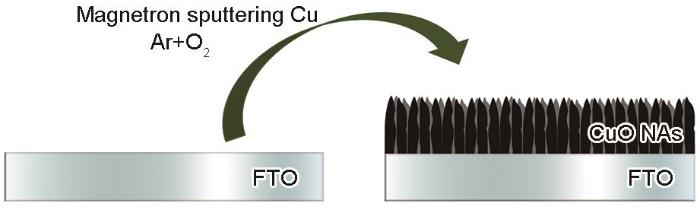
以Cu靶为反应物,使用直流电源溅射,在Ar和O2的气氛中改变FTO基底和磁控溅射腔体内的温度用原位热氧化方式磁控溅射出梭形CuO纳米阵列(CuO NAs)。梭形CuO NAs光阴极的制备流程,如图1所示。
图1
基体原位加热反应磁控溅射制备CuO纳米阵列(CuO NAs),是将暴露面积为1 cm2的FTO导电玻璃放置在磁控溅射模板上,使用磁控溅射设备中的直流电源在Ar和O2的气氛中溅射Cu靶(纯度:99.995%,尺寸:ϕ50.8×3 mm)对基片镀膜。氧分压为6%~94%,气体总流量为80 sccm。靶材与镀膜模板的距离约为10 cm,溅射功率恒为150 W,溅射时间为90 min。加热灯温度为300℃,工作压力为1.0 Pa。溅射时,改变CuO NAs的晶体取向、形貌及厚度,控制氧分压为50%,调控加热灯温度为100~500℃,溅射时间为15~120 min,工作压力为1.0 Pa,其他参数保持不变。为了调控CuO NAs电子结构,参数为溅射功率恒定为150 W,溅射时间为90 min,氧分压为50%,加热灯温度为400℃,工作压力为1.0~8.5 Pa。
使用极高分辨场发射扫描电子显微镜(SEM)观察样品表面和截面的微观形貌;使用型号为D8 Discover的X射线衍射分析仪(XRD)分析样品的晶体结构;使用型号为Escab-250的X射线光电子能谱仪(XPS)分析样品表面的化学成分和元素状态;使用紫外可见吸收光谱仪测试薄膜CuO光电极样品的光吸收,扫描的波长范围为200~1000 nm。
光电化学分解水及电化学特性的测试:测试光电流(CV曲线)时,使用石英电解槽作为测试容器,模拟太阳光光源为300 W的Xe灯,配备AM 1.5G的滤光片,光强调节为100 mW·cm-2。使用型号为EC-Lab VSP-300的电化学工作站中的三电极体系进行电化学测试,电解液为浓度为0.1 mol/L的KOH溶液(pH=13),工作电极为CuO光电极样品,对电极和参比电极分别为Pt片以及商业化Ag/AgCl电极(饱和),扫速为10 mV·s-1,斩波时间间隔为1 s。在电压为-0.4 V(相对于Ag/AgCl参比电极)的恒电位条件下测试电流-时间(I-T曲线),测试时间根据样品的光电流密度衰减程度而定。根据测试时间和衰减速度选定斩波时间间隔,一般以1 min或5 min为一个时间节点,使用的电解液,为浓度为0.1 mol/L的KOH溶液(pH=13)。使用电解液为0.1 mol/L Na2SO4溶液(pH=7)测试莫特肖特基曲线(M-S曲线),交流频率为1000 Hz。
2 结果和讨论
2.1 薄膜表面的形貌和结构
控制氧分压分别为6%,25%,50%,75%和94%溅射出系列CuO薄膜,研究氧分压对成膜的形貌和组成相的影响。图2给出了在不同氧分压下制备的薄膜的SEM照片。可以看出,在6%的氧分压下样品成蓬松的海绵状,厚度为15.50 μm,表面疏松多孔。氧分压为25%的样品呈块状,并未形成良好的晶体形貌,薄膜厚度为4.90 μm。氧分压为50%~94%的样品呈现出较好的晶体形貌。氧分压为50%的样品有充分生长的鳞状结构。氧分压为50%的样品其厚度为1.80 μm。充分生长的鳞状结构,可能为光电化学化学反应提供更多的反应位点。
图2

图2
氧分压不同的样品及其截面的SEM照片
Fig.2
SEM images of samples fabricated under different oxygen partial pressure (a~e) the oxygen partial pressure was 6%, 25%, 50%, 75% and 94%, respectively, (f~j) corresponding cross-section pictures and the thickness of different samples was provided
图3给出了XRD谱的数据结果。可以看出,氧分压为6%的的样品其成分以Cu和Cu2O为主,意味着Cu的不完全氧化。氧分压为25%的样品,其成分以Cu2O和CuO为主。因为薄膜较厚,基底FTO的衍射峰被掩盖,而Cu2O的生成也意味着反应发生在欠氧环境中。高于50%的O2分压就足以使反应在富氧条件下发生,制备出的CuO光阴极具有较高的结晶度,主峰为(11
图3
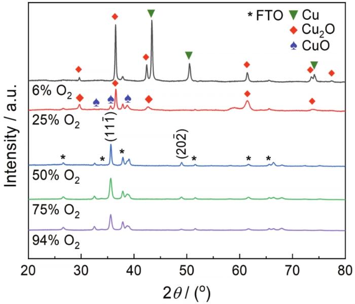
图3
压力为1.0 Pa、基底温度为300oC,氧分压分别为6%,25%,50%,75%,94%样品的XRD谱
Fig.3
XRD patterns of samples fabricated under the condition of a pressure of 1.0 Pa, the substrate temperature of 300oC, oxygen partial pressure of 6%, 25%, 50%, 75%, 94%, respectively
改变腔体内加热灯丝的温度,可调控FTO基片和腔内的温度(反应温度)。图4给出了在不同温度下制备的样品的SEM照片。可以看出,温度为200~300℃的CuO Nas其顶端具有明显的鳞状结构;温度为200℃制备的样品其鳞状结构更加小而致密;温度为300℃的样品其鳞状结构大而完整;温度为400℃的样品其侧面呈羽毛状,顶端尖锐,侧边有锯齿;温度为500oC的样品最光滑平整。温度为300℃制备的样品,其厚度最小。
图4
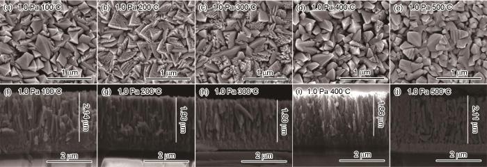
图4
压力为1.0 Pa,基底温度分别为100℃,200℃,300℃,400℃,500℃的CuO NAs光阴极及其截面的SEM照片
Fig.4
SEM images of samples fabricated under the condions of pressure of 1.0 Pa and substrate set temperatures of 100℃, 200℃, 300℃, 400℃, 500℃, respectively (a~e), and corresponding cross-section pictures (f~j) and the thickness of different samples was provided
图5给出了对样品的XRD分析结果。可以看出,在不同温度区间内CuO薄膜的晶体生长取向不同。温度为100~300℃制备的样品以(11
图5
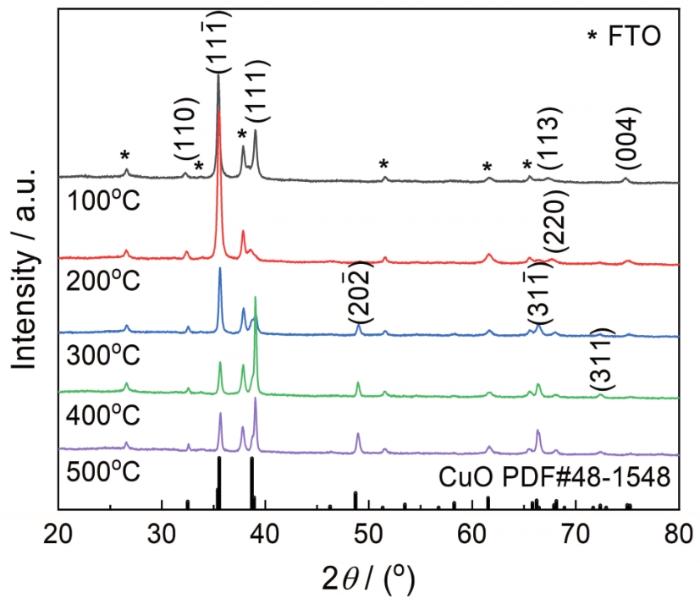
图5
压力为1.0 Pa,基底温度分别为100℃,200℃,300℃,400℃,500℃的CuO NAs光阴极的XRD谱和CuO的标准卡片
Fig.5
XRD patterns of samples fabricated under the conditions of pressure of 1.0 Pa and substrate temperatures of 100℃, 200℃, 300℃, 400℃, 500℃, respectively
图6
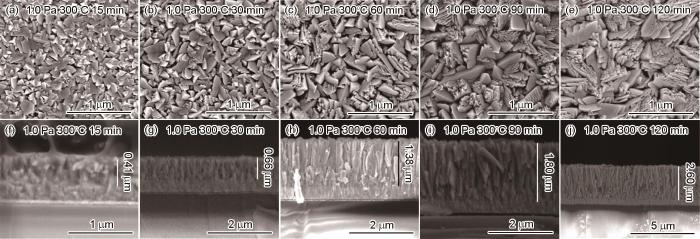
图6
压力为1.0 Pa、基底温度为300℃、溅射时间分别为15 min、30 min、60 min、90 min、120 min的CuO NAs光阴极及其截面的SEM照片
Fig.6
SEM images of CuO NAs photocathodes fabricated under the condition of a pressure of 1.0 Pa and the substrate temperature of 300℃ (a~e) the samples of different sputtering time, 15 min, 30 min, 60 min, 90 min, 120 min, respectively and (f~j) corresponding cross-section pictures, the thickness of different samples was provided
图7
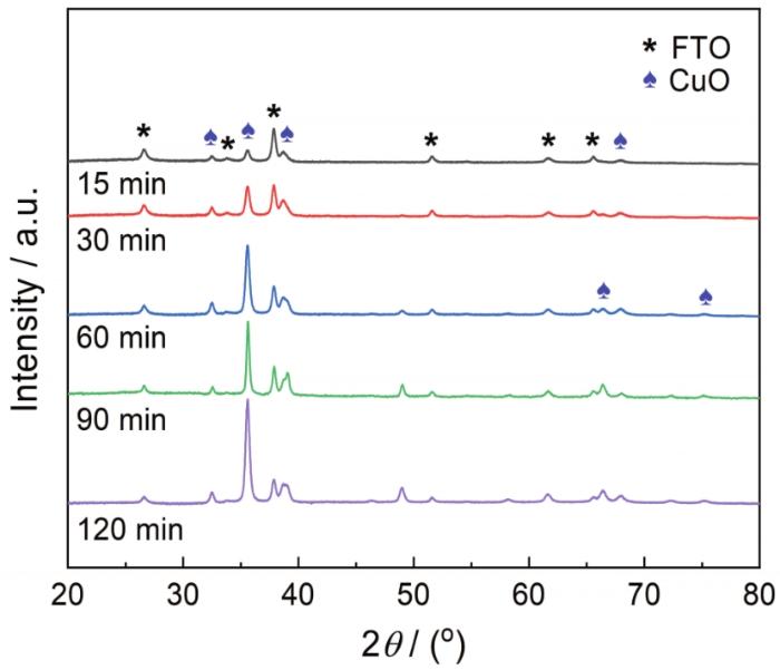
图7
压力为1.0 Pa,基底温度为300℃、溅射时间分别为15 min,30 min,60 min,90 min,120 min的CuO NAs光阴极的XRD谱
Fig.7
XRD patterns of the CuO NAs photocathodes fabricated under the condition of a pressure of 1.0 Pa and the substrate temperature of 300℃ but of different sputtering time, 15 min, 30 min, 60 min, 90 min, 120 min, respectively
为了研究制备压力对CuO NAs生长及性能的影响,在1.0~8.5 Pa范围内改变压力制备出一系列样品。样品和截面的SEM形貌表明,压力为1.0 Pa的样品最厚,具有最好的晶体形貌,呈梭状生长且结构更为松散,呈纳米阵列排布。随着制备压力的提高CuO Nas的膜厚逐渐减小并且纳米阵列的结构逐渐模糊。随着制备压力的提高,晶体的表面形貌变差(图8)。图9给出的XRD表征结果可进一步确认这一观察结果。同时,随着制备压力在1.5~1.0 Pa的变化,CuO NAs的主峰也发生了转变,从(11
图8

图8
基底温度为400℃,溅射时间为90 min,压力分别为1.0 Pa、1.5 Pa、4.1 Pa、8.5 Pa的CuO NAs光阴极及其截面的SEM照片
Fig.8
SEM images of CuO NAs photocathodes fabricated under the condition of a substrate temperature of 400℃, sputtering time of 90 min (a~d) working pressure was 1.0 Pa, 1.5 Pa, 4.1 Pa, 8.5 Pa, respectively, (e~h) corresponding cross-section pictures, the thickness of different samples was provided
图9
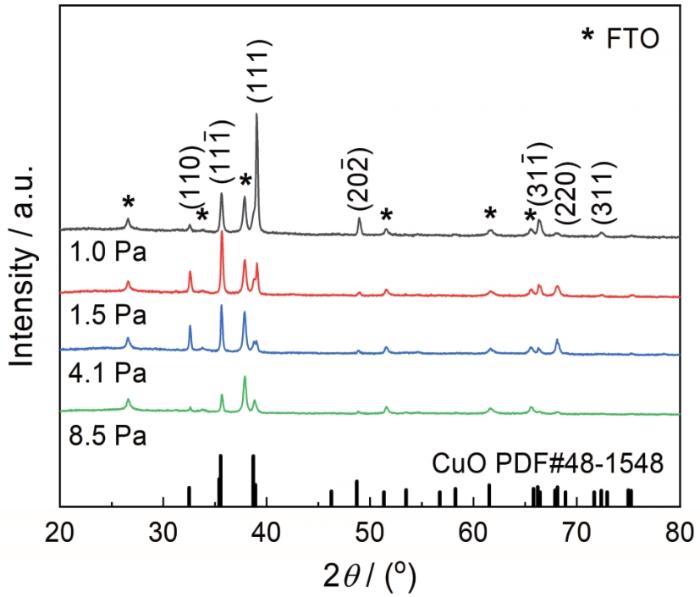
图9
基底温度为400℃,溅射时间为90 min,压力分别为1.0 Pa、1.5 Pa、4.1 Pa、8.5 Pa的CuO NAs光阴极的XRD谱
Fig.9
XRD patterns of CuO NAs photocathodes fabricated under the condition of a substrate temperature of 400℃, sputtering time of 90 min, working pressure of 1.0 Pa, 1.5 Pa, 4.1 Pa, 8.5 Pa, respectively
2.2 薄膜的吸收光谱
图10
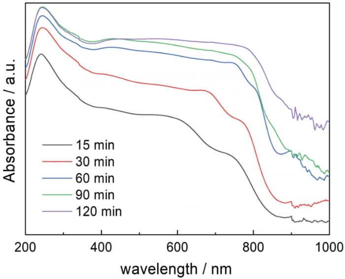
图10
制备压力为1.0 Pa,基底设定温度为300℃,溅射时间分别为15 min、30 min、60 min、90 min、120 min的CuO NAs光阴极的紫外和可见光吸收谱
Fig.10
UV-visible absorption spectra of the CuO NAs photocathodes fabricated under the condition of a pressure of 1.0 Pa and the substrate temperature of 300℃, sputtering time of 15 min, 30 min, 60 min, 90 min, 120 min, respectively
图11
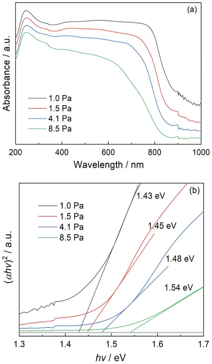
图11
基底温度为400℃,溅射时间为90 min,压力分别为1.0 Pa、1.5 Pa、4.1 Pa、8.5 Pa的CuO NAs光阴极的紫外和可见光吸收谱以及对应的Tauc图
Fig.11
UV-visible absorption spectra (a) and Tauc plot of the CuO NAs photocathodes fabricated with a condition of a sputtering time of 90 min and the substrate temperature was set at 300℃ but of different working pressure of 1.0 Pa, 1.5 Pa, 4.1 Pa, 8.5 Pa, respectively (b)
2.3 薄膜光电化学分解水的性能
图12给出了在不同氧分压下制备的样品在0.1 mol/L KOH溶液中的光电化学测试结果和在斩波条件下对应的LSV曲线。由图12并结合XRD分析结果,氧分压为6%的样品其成分以Cu为主,因此没有光响应能力。氧分压为25%的薄膜样品虽然以CuO和Cu2O为主,但是其厚度(4.90 μm)远远超过了其载流子传输距离,且其较差的结晶度和块状结构都不利于光生载流子的分离,因此其光响应也很弱。氧分压高于50%的样品,其光响应迅速提高。其原因是,高浓度的氧有利于合成p型CuO,且富氧条件有利于生成铜空位从而提高受主掺杂浓度(Na)。氧分压为50%下制备的样品具有最高的光电流密度,其最大光电流密度在0.4 V时(vs. RHE)达到了2.4 mA·cm-2。
图12
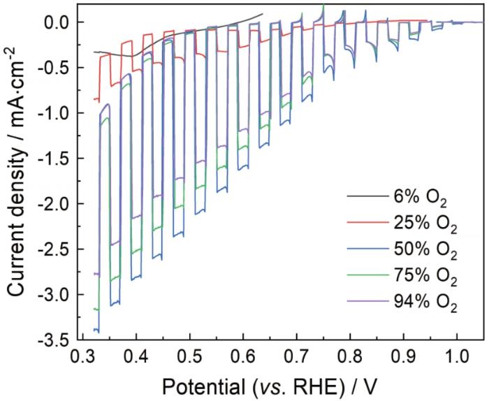
图12
压力为1.0 Pa,基底温度为300℃,氧分压分别为6%、25%、50%、75%、94%样品的光电流密度随施加电压的变化,电解液为0.1 mol/L KOH水溶液,电极面积为1 cm2
Fig.12
Applied potential bias-dependent photocurrent density curves of samples fabricated under the condition of a pressure of 1.0 Pa and the substrate temperature of 300℃, oxygen partial pressure of 6%, 25%, 50%, 75%, 94%, measured in 0.1 mol/L KOH aqueous solution and the area of photoelectrode was 1 cm2
图13
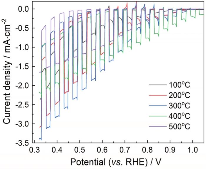
图13
压力为1.0 Pa、基底温度分别为100℃、200℃、300℃、400℃、500℃的CuO NAs光阴极的光电流密度与施加电压的关系,电解液为0.1 mol/L KOH水溶液,电极面积为1 cm2
Fig.13
Applied potential bias-dependent photocurrent density curves of samples fabricated under the conditions of pressure of 1.0 Pa, substrate temperatures of 100℃, 200℃, 300℃, 400℃, 500℃, respectively, measured in 0.1 mol/L KOH aqueous solution, the area of photoelectrode was 1 cm2
图14

图14
压力为1.0 Pa,基底温度为300℃,溅射时间分别为15 min、30 min、60 min、90 min、120 min的CuO NAs光阴极的光电流密度与电压的关系,电解液为0.1 mol/L KOH水溶液,电极面积为1 cm2
Fig.14
Applied potential bias-dependent photocurrent density curves of the CuO NAs photocathodes fabricated under the conditions of a pressure of 1.0 Pa and the substrate temperature of 300℃, sputtering time of 15 min, 30 min, 60 min, 90 min, 120 min, respectively, measured in 0.1 mol/L KOH aqueous solution, the area of photoelectrode is 1 cm2
测试了不同结晶度和晶面暴露样品的光电化学分解水性能。结果表明,线性极化(LSV)曲线表征了光电流密度的大小,纵深的纳米阵列结构可提高光吸收强度从而实现更高的能量利用率。同时,纳米阵列结构比平面结构提供了更多可能的活性位点。光生载流子沿着垂直轴线的方向转移,从而不受到载流子迁移长度的限制。压力为1.0 Pa和1.5 Pa的样品均具有较好的纳米阵列结构,在本对照组内光电流最大(1.83 mA·cm-2)(图15a),可能与其(11
图15
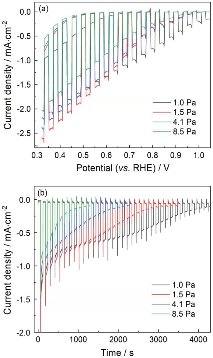
图15
基底定温度为400℃,溅射时间为90 min,压力分别为1.0 Pa、1.5 Pa、4.1 Pa、8.5 Pa的CuO NAs光阴极的线性极化曲线和光电流随时间的变化,电解液为0.1 mol/L KOH水溶液,电极电位为0.56 V(vs. RHE),电极面积为1 cm2
Fig.15
Applied potential bias-dependent photocurrent density curves (a) and Time dependent photocurrent density curves (b) of CuO NAs photocathodes fabricated under the conditions of a substrate temperature of 400℃, sputtering time of 90 min, pressure of 1.0 Pa, 1.5 Pa, 4.1 Pa, 8.5 Pa, respectively, measured in 0.1 mol/L KOH aqueous solution at 0.56 V (vs. RHE), the area of photoelectrode was 1 cm2
2.4 讨论
因为CuO光阴极中的电荷分离较难,通过原位基体加热反应磁控溅射制备了具有更强光捕获能力和载流子分离和转移能力的CuO NAs光阴极,通过控制氧分压、基底温度、制备压力以及溅射时间制备了具有不同相组成、晶体形貌、晶体生长取向、晶面暴露、厚度以及电子结构的CuO NAs光阴极。优化的CuO NAs光阴极其光电流密度达到2.4 mA·cm-2(0.4 V vs. RHE)。在此过程中,通过观察不同样品的微观形貌和电化学测试,探究了优化光电化学性能的原因。1. 高于25%的氧分压可制备出纯CuO相,氧分压为50%的样品具有最好的结晶度,从而与同一对照组其他样品相比其光电流密度最高;2. 样品的基底温度在100℃~500℃变化时,以300℃为转变点其样品的主峰晶面从(11
为了进一步理解不同光电极间光电化学行为的差异,根据莫特-肖特基(Mott-Schottky)曲线测量了在不同压力下样品的平带电位和载流子浓度(图16)。根据莫特-肖特基关系式
计算出施主浓度。其中
图16
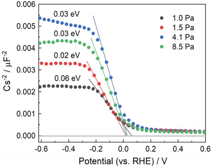
图16
基底温度为400℃、溅射时间为90 min、制备压力分别为1.0 Pa、1.5 Pa、4.1 Pa和8.5 Pa的CuO NAs光阴极的莫特-肖特基曲线
Fig.16
Mott-Schottky curves of the CuO NAs photocathodes fabricated under the condition of a sputtering time of 90 min, the substrate temperature of 300℃, pressure of 1.0 Pa, 1.5 Pa, 4.1 Pa, 8.5 Pa, respectively
3 结论
(1) 用原位基体加热反应磁控溅射方法可制备一种CuO阵列结构,改变氧分压、溅射时间、工作压力和基底温度可制备具有不同晶体取向结构和电子结构的CuO纳米阵列结构光阴极。
(2) 较高的氧分压(50%)有利于制备纯相p型CuO光电极。暴露(11
(3) 改变制备压力可调控p型CuO光阴极的电子结构从而提高其性能,在尽可能的低压(1.0 Pa)条件下能制备出最优光电化学分解水性能。优化后的CuO 纳米阵列光阴极在0.4 V (vs. RHE)条件下其光电流密度可达2.4 mA·cm-2。
参考文献
Stable unassisted solar water splitting on semiconductor photocathodes protected by multifunctional GaN nanostructures
[J].
Crystallographic-orientation-dependent charge separation of BiVO4 for solar water oxidation
[J].
Monolithic photoelectrochemical device for direct water splitting with 19% efficiency
[J].
Wind energy
[J].
Water photolysis at 12.3% efficiency via perovskite photovoltaics and Earth-abundant catalysts
[J].
Basic principles, diverse forms of implementations and emerging scientific opportunities
[J].
Solar-to-hydrogen energy conversion based on water splitting
[J].
A review of direct Z-scheme photocatalysts
[J].
Heterogeneous molecular systems for photocatalytic CO2 reduction with water oxidation
[J].
Metal-doped Mo2C (metal = Fe, Co, Ni, Cu) as catalysts on TiO2 for photocatalytic hydrogen evolution in neutral solution
[J].
金属(Fe,Co,Ni,Cu)掺杂的Mo2C催化剂在TiO2表面用于中性条件光催化分解水产氢
[J].
Odd‐membered cyclic hetero‐polyoxotitanate nanoclusters with high stability and photocatalytic H2 evolution activity
[J].
具有高稳定性以及光催化产氢活性的奇数环状异金属钛氧纳米团簇
[J].
Recent strategies to enhance the efficiency of hematite photoanodes in photoelectrochemical water splitting
[J].
提高氧化铁光电催化分解水效率的策略进展
[J].
Hydrothermal synthesis and photocatalytic activity of CuO/ZnO composite photocatalyst
[J].
CuO/ZnO复合光催化剂的制备和性能
[J].
Influence of heat treatment on photocatalytic activity of Ag-ZnO heterostructure
[J].
热处理对Ag-ZnO异质结构光催化性能的影响
[J].
用溶胶-凝胶法制备纯ZnO和Ag修饰ZnO复合光催化剂,并分别对其进行了400℃、450℃、500℃保温2 h的热处理。使用XRD、SEM、TEM、XPS、PL、BET等手段对其进行了表征。结果表明,纯ZnO和Ag修饰ZnO均为六方纤锌矿晶型,Ag颗粒沉积在ZnO表面形成了Ag-ZnO异质结构。以罗丹明B为目标污染物研究了样品的光催化活性。结果表明,热处理温度对纯ZnO的光催化性能的影响较大,在450℃热处理后光催化效果最佳;热处理温度对Ag修饰ZnO的光催化性能没有显著的影响;Ag修饰ZnO比纯ZnO的光催化活性均有所提高,因为Ag修饰提高了ZnO表面羟基的含量并抑制了光生电子与空穴的复合。在500℃热处理后Ag修饰ZnO对罗丹明B的60 min降解率达到98%,其反应速率常数为0.063 min<sup>-1</sup>。
Nanocrystalline CuO thin films: synthesis, microstructural and optoelectronic properties
[J].
Identifying copper vacancies and their role in the CuO based photocathode for water splitting
[J].
Stabilized solar hydrogen production with CuO/CdS heterojunction thin film photocathodes
[J].
Efficient solar water splitting photocathodes comprising a copper oxide heterostructure protected by a thin carbon layer
[J].
J. Semiconductor Electrodes: X. Photoelectrochemical behavior of several polycrystalline metal oxide electrodes in aqueous solutions
[J].
J. Zone-center (q=0) optical phonons in CuO studied by Raman and infrared spectroscopy
[J].
The effect of hydrostatic pressure on the ambient temperature structure of CuO
[J]. J.
Fabrication of films of Co doped TiO2 nanotube array and their photocatalytic reduction performance
[J].
钴掺杂TiO2纳米管阵列薄膜的制备及其光催化还原性能
[J].用磁控溅射法在ITO玻璃基底上制备Ti-Co合金薄膜,对其阳极氧化处理制备出钴掺杂TiO<sub>2</sub>纳米管阵列薄膜,研究了钴掺杂对纳米管阵列薄膜的形貌、结构、吸收光谱以及光催化还原性能的影响。结果表明:钴掺杂TiO<sub>2</sub>纳米管阵列薄膜为锐钛矿相,管状阵列的管径均一、排列规整。钴掺杂使薄膜形成(001)择优取向。随着钴掺杂量的提高,薄膜吸收可见光的能力提高。钴含量(原子分数)为0.19%的薄膜光催化性能最优,可见光照150 min后对Cr(VI)的还原率可达98.4%。
Effect of B and Ru co-modification on structure and photocatalytic activity of TiO2 nanotubes
[J].
B和Ru共改性对TiO2纳米管阵列的结构和光催化性能的影响
[J].
2D mesoporous ultrathin Cd0.5Zn0.5S nanosheet: Fabrication mechanism and application potential for photocatalytic H2 evolution
[J].
二维介孔超薄Cd0.5Zn0.5S纳米片:形成机制及光催化分解水制氢性能
[J].
Photocurrent enhancement of d.c. sputtered copper oxide thin films
[J].
S. Comparison of the device physics principles of planar and radial p-n junction nanorod solar cells
[J].
A. Diffusion length measurement and silicon quality
[J].
Molybdenum tungsten disulfide with a large number of sulfur vacancies and electronic unoccupied states on silicon micropillars for solar hydrogen evolution
[J].
p-Type InP nanopillar photocathodes for efficient solar-driven hydrogen production
[J].
Semiconductor Nanowires for Energy Conversion
[J].
Cu2O nanowire photocathodes for efficient and durable solar water splitting
[J].
