
文献标识码: 分类号 O484 文章编号 1005-3093(2016)08-0634-07
收稿日期: 2015-11-2
网络出版日期: 2016-09-28
版权声明: 2016 《材料研究学报》编辑部 《材料研究学报》编辑部
基金资助:
展开
摘要
根据磁控溅射金属铜膜在超声清洗中从硅基底上发生剥落的现象, 分析了样品在声场中的运动和受力状态, 发现样品会发生受迫振动, 拉-拉周期应力引起膜基界面的失效是薄膜脱落的主要原因, 而空化作用是次要原因。通过建立的力学模型, 计算了膜基结合强度。与划痕法等所测得的膜基结合强度值的比较, 计算值与测量值在数量级和与溅射参数变化趋势上有很好的吻合。此评价方法可以应用于溅射铜膜/多晶金刚石的膜基体系上, 并研究了超声参数、基底表面形貌、基底成份等因素对膜基结合强度的影响。
关键词:
Abstract
As magnetron sputtering copper films would flake from silicon substrates in the ultrasonic cleaner, this paper analyzed the states of motion and stress of samples in the ultrasonic medium. By calculation, it was found that the tension-tension cycle stress caused by forced vibration was the main reason of interface damage. Then the ultrasonic mechanical model was established and the film-substrate adhesive strength was calculated. The results showed that the adhesive strength values gotten by the ultrasonic test method were in the same order of magnitude compared with that of scratch test results. In addition, this ultrasonic test method was used to test adhesion of copper films on diamond substrates. The influence of ultrasonic parameters, substrate morphology as well as composition on adhesive strength was also discussed.
Keywords:
在微电子领域, 半导体材料的表面金属化是制备半导体器件的重要工艺环节, 而金属膜与基底的结合力是器件各种性能得以发挥的基础[1-3]。磁控溅射是半导体表面金属化经常采用的工艺, 借助掩模和光刻技术可以实现各种电极结构的大面积成型, 因此在微电子领域得到广泛的应用[4, 5]。磁控溅射所获得的器件薄膜作为小尺寸薄膜材料, 受界面的影响更加明显, 力学性能与传统块体材料存在许多不同[6]。为测量薄膜与基底的结合强度, 开发了如划痕法, 四点弯曲法, 鼓膜法, 热应力法, 残余应力法, 拉拔法等等多种测试手段[7-13]。但这些方法都有其局限性, 或者对薄膜有限制, 或者需要破坏基底, 或者操作复杂, 目前还没有一种通用的测试方法。近年来, CVD金刚石得到了越来越多的重视, 器件化成为其在电子领域应用的一个重要的研究内容[14-16]。由于金刚石的特殊性, 上述常用的表征膜基结合强度方法限制颇多。因此, 急需提出一种切实可行的评价方法。在微电子器件生产过程中, 超声清洗是被广泛采用的一种清洁技术, 但是对于膜基结合强度不好的样品, 往往出现膜体剥落的失效现象。因此, 我们通过实验以及构建膜基体系在声场中的力学模型, 分析膜基界面处的受力状态, 探讨采用超声的方法来表征和评价样品的膜基结合强度的力学依据, 并尝试其在金属膜/金刚石体系上的应用, 以评估采用超声方法评价膜基结合强度的可行性。
使用JCP-200磁控溅射镀膜机制备薄膜, 靶材为高纯铜(99.999%), 工作气体为高纯氩气(99.99%)。基底使用单晶硅片和多晶金刚石片, 面积均为10 mm×10 mm, 硅片厚度为300 μm, 表面粗糙度约0.4 nm。金刚石厚度为500 μm, 表面粗糙度分别为13.8 nm(经抛光), 168.2 nm, 19 μm。在进行溅射沉积铜膜之前, 对两种基底进行表面处理, 将基底依次置于盐酸、丙酮、酒精、去离子水中各超声清洗10 min, 清洗完成后使用电热板加热至100℃烘烤30 min。然后使用磁控溅射镀膜机制备薄膜样品。各样品沉积工艺参数如表1所示。所得薄膜厚度不同, 但均在数百纳米范围。
表1 溅射参数及对应样品
Table 1 Parameters of sputtering of corresponding samples
| Sample | Si-1 | Si-2 | Si-3 | Polished | Fine-grain | Coarse-grain |
|---|---|---|---|---|---|---|
| Substrate | Si | Si | Si | Diamond | Diamond | Diamond |
| Sputtering power/W | 250 | 375 | 425 | 425 | 425 | 425 |
| Pressure/Pa | 1.5 | 1.5 | 1.5 | 1.5 | 1.5 | 1.5 |
| Sputtering time/min | 8 | 8 | 8 | 8 | 8 | 8 |
硅基底的表面粗糙度使用NTEGRA Prime NT-MDT 原子力显微镜得到, 金刚石基底的表面粗糙度采用Marsurf 300C表面粗糙度仪得到。利用RigukuSmartLab X-Ray衍射仪测量金刚石基底的晶体结构, 角度范围20°~140°, 步长0.01。使用JobinYvon HR 800型共聚焦显微拉曼光谱仪测试其成分, 激光源波长532 nm, 扫描范围1000~2000 cm-1。样品的表面形貌使用KYKY-8000F场发射电镜表征。所使用的划痕仪器为Hysitron TI-900 TriboIndenter原位纳米力学测试系统(圆椎金刚石压头, 曲率半径1 μm), 最大载荷2 mN, 分辨率为0.5 μN, 针尖最大位移15 μm。
实验中使用的超声清洗设备功率为80 W, 频率为40 kHz, 功率密度0.33 W/cm2。水槽尺寸为长150 mm×宽140 mm×高150 mm。超声介质为去离子水, 室温下密度1000 kg/m3, 平衡蒸汽压2.34 kPa, 绝热系数1.33, 声速1500 m/s。水深约30 mm。
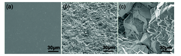
铜/硅膜基体系在进行超声清洗时发生了铜膜的剥落, 剥落面积随超声清洗时间的加长而变大, 最终全部剥离硅基底。采用SEM观察了这一膜体失效过程, 以Si-1样品为例, 结果见图1。Si-2、Si-3样品失效过程与之相似。
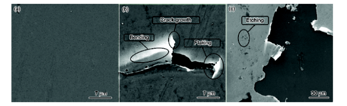
图1中可以看到, 没有超声清洗时, 磁控溅射得到的铜薄膜表面是平滑的(图1(a)); 随着超声处理时间的增加, 在平滑的铜膜表面上部分区域发生了破损, 出现了裂纹、褶皱和剥落(图1(b)), 随着超声时间的进一步延长, 爆发破损的区域增多, 剥落面积变大(图1(c))。由此表明, 铜膜的失效形式主要为碎裂和剥落, 而剥落是铜膜失效的最终形式。
图1 Si-1样品超声处理前后的表面铜膜形貌: (a)超声处理前; (b)超声处理1 min; (c)超声处理2 min。
Fig.1 Copper film morphology of sample Si-1 (a) before ultrasonic treatment , (b) ultrasonic treatment for 1 min and (c) 2 min
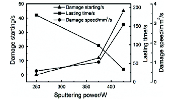
图2为溅射功率与硅基底样品上铜膜失效时间和剥落速度的关系。可以看到, 随着溅射功率的增大, 铜膜的剥落速度变大, 但是发生初始剥落的时间较晚, 整个铜膜全部剥落的总时长变短。文献指出: 随着溅射功率的提高, 入射原子的能量加大, 有利于减少薄膜内的缺陷, 致密度得到提高, 薄膜整体的机械性能变好[17-19]。因此可以解释实验中高溅射功率下制备的铜膜其发生初始剥落的时间被推后。但是溅射功率的提高也使得薄膜的内应力增加[20], 一旦膜基结合失效, 膜体应力的释放会促进裂纹在膜基界面处的扩展, 导致薄膜更快的脱落。这也与我们的实验现象吻合。
图2 溅射功率与铜膜失效时间和剥落速度的关系
Fig.2 Relationship of sputtering powers with damage time and speed
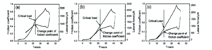
对硅基底样品进行纳米划痕测试, 并计算膜基结合强度。样品划痕测试结果如图3所示。由划痕结果可知各样品的膜基结合力分别为: 1207 μN、1160 μN和840 μN。利用Hertz公式[21]得到的Hertz结合强度分别为: 10.4 MPa、10.1 MPa和8.6 MPa。
图3 (a)Si-1样品(b)Si-2样品(c)Si-3样品的纳米划痕结果
Fig.3 Nano-scratch test results of (a) sample Si-1, (b) sample Si-2 and (c) sample Si-3
2.3样品在超声场中的应力分析
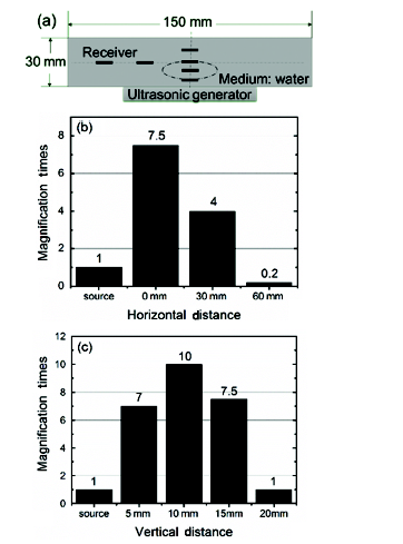
样品在超声处理时, 受到声场的声压和介质空化作用的双重影响。图4(a)是超声清洗槽和超声振荡源的几何模拟模型, 其中超声振荡源发出的是纵波, 介质为纯水。利用wave2000软件计算了两组不同位置的声压, 第一组的位置为: 距离底面15 mm处, 偏离中心0 mm、30 mm和60 mm; 第二组的位置为: 沿中线距底面5 mm、10 mm、15 mm和20 mm。分别在图4(a)中进行了标示。设振荡源处的声压幅值为1, 模拟得到的声压幅值与位置的关系如图4(b)和4(c)所示。可见在超声场中声压幅值分布不同, 介质中心偏下靠近波源的区域声压幅值是最大的。
图4 (a)超声模拟模型。假定振荡源处声压幅值为1时(b)距离底面15 mm的水平面内, 距离中轴线0 mm, 30 mm, 60 mm处接收到的声压幅值(c)中轴线上距离底面5 mm, 10 mm, 15 mm, 20 mm处接收到的声压幅值
Fig.4 (a) Ultrasonic simulation model. Supposing acoustic pressure amplitude (APA) of wave source to be 1, (b) 15 mm above bottom, APA values away from the central axis 0 mm, 30 mm, 60 mm and (c) along central axis, APA values of 5 mm, 10 mm, 15 mm, 20 mm above bottom
需要指出的是在声场中各模拟计算点只受到纵向的声波作用[22]。
对于空化作用, 空化泡溃灭时的最大压强为[23]
其中, Pm为空化泡溃灭过程中受到外界的总压强; Pv为介质平衡蒸汽压;
对于声场作用, 周期性的声场振动引起介质的疏密变化造成声压Pa, 而声压幅值PA可以认为是样品单位面积受到的最大压力, 其表达式为
其中, I表示功率密度,
由于声压是周期变化的, 样品在超声场中会发生受迫振动, 则样品的振动方程可表示为[25]:
通解为
其中, X为振动位移; m为样品质量; -kx为弹性力;
由于膜体与基底材料不同, 约束方式也不同, 薄膜与基底的位移幅值是不同的, 以角标f表示薄膜, s表示基底, 则二者的位移幅值之差Δx为:
另外, 二者振动的位相也有差异, 表示为:
由此可知在超声场中, 薄膜与基底的振动位相存在差异, 导致振动不同步, 造成薄膜与基底之间存在着拉-拉周期应力作用, 界面在循环应力的作用下可以发生疲劳失效。另外, 研究表明, 循环应力也会引起薄膜的疲劳, 造成金属薄膜裂纹的萌生和发展[26-28], 有利于薄膜的失效。
设原子间相互作用势为U, 间距为r, 则kf=d2U/dr2, 根据Morse势能公式及Cu-Si结合的相关参数[29], 可得平衡位置Cu-Si的kf为35.5 N/m。将kf的数值及样品数据带入公式(5)和(6), 发现Δx∝PAS/ω。
由此给出声场中的膜基界面结合强度σ的表示为:
其中系数α是超声能量传递的效率, n是与膜基结合界面缺陷有关的系数, S是剥落薄膜的面积。薄膜与基底质量应有较大差距。考虑到循环应力条件下, 应力过小时失效难以发生, 因此x应当取分数。
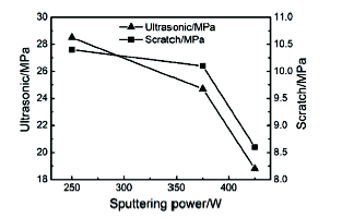
对于本实验条件下的完整连续薄膜, 取n=1m-2, α=0.5, x=1/4, 则Si-1~Si-3号样品膜基结合强度分别为28.5 MPa, 24.7 MPa, 18.8 MPa, 与纳米划痕法得到的数据相近, 且随溅射功率变化的趋势也与划痕法的结果类似, 如图5所示。因此超声方法检测膜基结合强度是可行的。由(7)式也可以得到超声参数对膜基结合强度的影响。
图5 分别使用超声方法与划痕法得到的膜基结合强度
Fig.5 Adhesive strength curves by ultrasonic method and scratch test
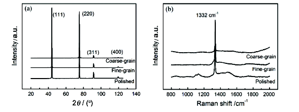
采用化学气相沉积技术制备的金刚石多晶自支撑膜的表面形貌如图6所示, 其中图6(a)为抛光样品表面; 图6(b)为细晶样品表面, 晶粒较细小; 图6(c)为粗晶样品表面, 晶粒粗大。其晶体结构和成份分别采用XRD和Raman技术进行检测, 所得结果如图7所示。XRD可以表征晶体种类, 同一样品不同晶向的强度比值可以表征晶粒的择优取向。如图7(a)所示, 抛光样品与细晶样品都是(111)晶面占优, 而粗晶样品占优晶面为(220)。而Raman结果中1332cm-1峰代表金刚石相, 是碳原子sp3杂化造成的, 而1357~1580 cm-1峰代表杂质相, 是碳原子sp2杂化造成的[30]。因此二者比值可以定性地对比金刚石样品杂质的多少[31]。根据图7(b)可得抛光样品, 细晶样品, 粗晶样品sp3/sp2的数值分别为7.9, 14.5, 4, 可见细晶样品中杂质含量最少。
图6 不同金刚石基底的表面形貌(a)抛光样品(b)细晶样品(c)粗晶样品
Fig.6 Morphologies of different diamond substrates (a) polished sample, (b) fine-grain sample and (c) coarse-grain sample
图7 金刚石基底的(a)XRD结果和(b)拉曼结果
Fig.7 (a) XRD and (b) Raman patterns of diamond substrates
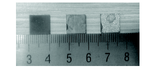
按照表1的参数在金刚石表面溅射沉积铜膜, 然后进行超声处理, 60 min后, 样品的外观如图8所示。可以看到, 抛光样品表面的铜膜全部脱落, 细晶样品表面几乎没有破损, 粗晶样品铜膜在四角有微小的剥落。
图8 超声处理60 min后各样品的外观(其中的弧形区域为夹具形状): (a)抛光样品(b)细晶样品(c)粗晶样品
Fig.8 Appearance of each sample after ultrasonic cleaning for 60min (the arc part on each sample is the shape of fixture): (a) polished sample, (b) fine-grain sample, (c) coarse-grain sample
样品超声处理的各项数据如表2所示。细晶样品没有剥落, 无法计算结合强度。由公式(7)计算得到抛光和粗晶样品的膜基结合强度分别为58.7 MPa和102.4 MPa。该结果与粘接-拉拔方法得到的类似界面的结合数据范围相同[32]。但粗晶样品剥落位置特殊, 有可能使计算结果发生失真。结合XRD和Raman数据, 可知基底表面成分对膜基结合强度影响不明显, 而基底形貌对膜基结合强度有较大影响。
表2 铜膜在金刚石基底上的失效时间和超声法获得的膜基结合强度
Table 2 Failure time and ultrasonic adhesive strength of diamond substrates with copper films
| Sample | Polished | Fine-grain | Coarse-grain |
|---|---|---|---|
| Damage starting time/s | 360 | - | 2400 |
| Lasting time/s Damage speed/mm2/s | 3240 0.03 | - - | 1200 0.003 |
| Adhesive strength/MPa | 58.7 | - | 102.4 |
在半导体加工制造中, 需要进行金属化处理的表面对粗糙度有很高的要求[33-35], 因此细晶和粗晶样品的粗糙度过大, 检测膜基结合强度没有实际意义。从实验结果看, 在合适的粗糙度范围内, 超声方法可以方便的表征样品的膜基结合强度。
1. 在超声清洗中, 溅射铜膜/单晶硅膜基体系以薄膜剥落为最终失效形式。SEM观察发现, 薄膜失效经历了碎裂-褶皱-剥落的过程。随着溅射功率的增加, 薄膜剥落初始时间延后, 剥落速度变快。
2. 声场模拟显示, 超声场中声压幅值最大区域位于介质中心偏下。由于薄膜和基底对声场激励的响应存在位相差, 导致膜基界面承受拉-拉周期应力, 是膜体剥落失效的主要原因。而空化作用的最大应力低于铜膜的屈服强度, 对膜基剥落失效起次要作用。
3. 提出了超声检测膜基结合强度的计算公式,
The authors have declared that no competing interests exist.
| [1] |
Adhesion and material transfer between contacting Al and TiN surfaces from first principles,
A series of density functional theory (DFT) simulations was performed to investigate the approach, contact, and subsequent separation of two atomically flat surfaces consisting of different materials. Aluminum (Al) and titanium nitride (TiN) slabs were chosen as a model system representing a metal-ceramic interface and the interaction between soft and hard materials. The approach and separation were simulated by moving one slab in discrete steps normal to the surfaces allowing for electronic and atomic relaxations after each step. Various configurations were analyzed by considering (001), (011), and (111) surfaces as well as several lateral arrangements of these surfaces at the interface. Several tests were conducted on the computational setup, for example, by changing the system size or using different approximations for the exchange correlation functional. The performed simulations revealed the influences of these aspects on adhesion, equilibrium distance, and material transfer. These interfacial properties depend sensitively on the chosen configuration due to distinct bond situations. Material transfer, in particular, was observed if the absolute value of the adhesion energy for a given configuration is larger than the energy cost to remove surface layers. This result was found to be independent of the employed exchange correlation functional. Furthermore, it was shown that a simple comparison of the surface energies of the slabs is not sufficient to predict the occurrence of material transfer.
|
| [2] |
Physics of adhesion,
Adhesion physics was relegated to the lowest echelons of academic pursuit until the advent of three seemingly disconnected events. The first, atomic force microscopy (AFM), eventually allowed fine-scale measurement of adhesive point contacts. The second, large-scale computational materials science, now permits both hierarchical studies of a few thousand atoms from first principles or of billions of atoms with less precise interatomic potentials. The third is a microelectronics industry push towards the nanoscale which has provided the driving force for requiring a better understanding of adhesion physics. In the present contribution, an attempt is made at conjoining these separate events into an updating of how theoretical and experimental approaches are providing new understanding of adhesion physics. While all material couples are briefly considered, the emphasis is on metal/semiconductor and metal/ceramic interfaces. Here, adhesion energies typically range from 1 to 100 J mwhere the larger value is considered a practical work of adhesion. Experimental emphasis is on thin-film de-adhesion for 10 to 1000 nm thick films. For comparison, theoretical approaches from first principles quantum mechanics to embedded atom methods used in multi-scale modelling are utilized.
|
| [3] |
Review of recent advances in electrically conductive adhesive materials and technologies in electronic packaging,
Electrically Conductive Adhesives (ICAs: Isotropic Conductive Adhesives; ACAs: An-isotropic Conductive Adhesives; and NCAs: Non-conductive Adhesives) offer promising material solutions for fine pitch interconnects, low cost, low-temperature process and environmentally clean approaches in the electronic packaging technology. ICAs have been developed and used widely for traditional solder replacement, especially in surface mount devices and flip chip application. These also need to be lower cost with higher electrical/mechanical and reliability performances. ACAs have been widely used in flat panel display modules for high resolution, lightweight, thin profile and low power consumption in film forms (Anisotropic Conductive Films: ACFs) for last decades. Multi-layered ACF structures such as double and triple-layered ACFs were developed to meet fine pitch interconnection, low-temperature curing and strong adhesion requirements. Also, ACAs have been attracting much attention for their simple and lead-free processing as well as cost-effective packaging method for semiconductor packaging applications. High mechanical reliability, good electrical performance at high frequency level and effective thermal conductivity for high current density are some of required properties for ACF materials to be pursued for a wide usage in flip chip technology. Recently, NCAs are becoming promising for ultra-fine pitch interconnection and low cost joining materials in electronic packaging applications. In this paper, an overview of the recent developments and applications of electrically conductive adhesives for electronic packaging with focus on fine pitch capability, electrical/mechanical/thermal performance and wafer level packaging application is presented.
|
| [4] |
Simple lithographic approach for subwavelength structure antireflection,
A simple lithographic method is developed to generate large-area antireflective subwavelength structures (SWSs), in which the metal island films are used as masks. Using magnetron sputter deposition, stochastically arranged Ag islands were fabricated on Si substrates with dimensions controlled in the range of 50 鈭400 nm . After reactive ion etching with C F 4 , Si SWSs were formed, with the same arrangement and density as those of Ag islands. The measured reflectivity was decreased from 鈭40 % for polished Si to 鈭5 % for Si SWS surfaces. The residual reflection was thought to be mainly from the bottoms of 鈥淯鈥shape grooves.
|
| [5] |
High power pulsed magnetron sputtering: A review on scientific and engineering state of the art,
High power pulsed magnetron sputtering (HPPMS) is an emerging technology that has gained substantial interest among academics and industrials alike. HPPMS, also known as HIPIMS (high power impulse magnetron sputtering), is a physical vapor deposition technique in which the power is applied to the target in pulses of low duty cycle (less than10%) and frequency (less than10 kHz) leading to pulse target power densities of several kW cm(-2). This mode of operation results in generation of ultra-dense plasmas with unique properties, such as a high degree of ionization of the sputtered atoms and an off-normal transport of ionized species, with respect to the target. These features make possible the deposition of dense and smooth coatings on complex-shaped substrates, and provide new and added parameters to control the deposition process, tailor the properties and optimize the performance of elemental and compound films.
|
| [6] |
Progress in fatigue of small dimensional materials,
Small dimensional materials are widely used in micro/nano--systems, such as largescale integrated circuits and microelectromechanical systems (MEMS).Since the geometric and microstructural dimensions of thematerials are ranged from microns to nanometers,the constraints of the dimensions on dislocation activities and the effects ofsurfaces and interfaces in the small dimensional materials result in fatigue behaviors differentfrom that of the bulk materials. In this paper, fatigue testing methods,cyclic deformation, crack initiation and propagation behaviors of the small dimensional materials studied in recent years, such as thin films, are reviewed. The corresponding fatigue size effects and damage mechanisms are discussed. The prospective research directions of fatigue of small dimensional materials in the future are forecasted.
|
| [7] |
Interfacial toughness measurements for thin films on substrates,
<h2 class="secHeading" id="section_abstract">Abstract</h2><p id="">There are more than 200 different methods for measuring adhesion, suggesting it to be material, geometry and even industry specific. This availability has exploded at least partly due to the arrival of dissimilar material interfaces and thin films and the ease with which microfabrication techniques apply to silicon technology. Having an eye toward those tests utilized for thin films, this paper reviews only a few of these techniques. The emphasis is on measuring thin film adhesion from the standpoint of fracture mechanics, when the film is mechanically or by other means removed from the substrate, and the amount of energy necessary for this process is calculated per unit area of the removed film. This tends to give values approaching the true work of adhesion at small thickness and greater values of the practical work of adhesion at larger thickness, all being in the 30–30,000 nm range. The resulting large range of toughnesses is shown to be dependent on the scale of plasticity achieved as controlled by film thickness, microstructure, chemistry and test temperature.</p><p id="">While the tests reviewed largely address the measurement of elastic strain energy release rates, we also briefly address a few theoretical models which are specific to the resistance side of the delamination equation. The weight of the evidence suggests for ductile metallic films that the major extrinsic variables are film stress, extent of delamination, thickness and temperature while the major intrinsic ones are modulus, yield strength, the thermodynamic work of adhesion and one or more length scales. For some 25 film/substrate multilayers, with emphasis on Al, Au and Cu, the comparison of several theoretical models as to how the extrinsic and intrinsic variables intertwine is made.</p>
|
| [8] |
An overview of the potential of quantitative coating adhesion measurement by scratch testing,
The scratch test has been used to assess the adhesion of thin hard coatings for some time now and is a useful tool for coating development or quality assurance. However, the test is influenced by a number of intrinsic and extrinsic factors which are not adhesion-related and the results of the test are usually regarded as only semi-quantitative. The stress state around a moving indenter scratching a coating/substrate system is very complex and it is difficult to determine the stresses which lead to detachment. Furthermore, the interfacial defect state responsible for failure is unknown. However, by a careful analysis of the observed failure modes in the scratch test (not all of which are related to adhesion) it is possible to identify adhesive failures and in some cases these occur in regions where the stress state is relatively simple and quantification can be attempted. Ideally engineers would like a material parameter (such as work of adhesion or interfacial toughness) which can be used in an appropriate model of the coating-substrate system stress state to determine if detachment will occur under the loading conditions experienced in service. This data is not usually available and the development of such models must be seen as a long-term goal. In modem indentation and scratch systems the work of friction (or indentation) can be directly measured and the relationship between this parameter and adhesive failure can be demonstrated in some cases. This paper reviews the main adhesion-related failure modes and the stresses responsible for them and indicates where quantification is possible illustrating this with results from hard coatings on steel, thermally grown oxide scales and optical coatings on glass. The use of empirical calibration studies, directly measured work of friction and quantification by finite element methods is discussed.
|
| [9] |
Nanoindentating mechanical responses and interfacial adhesion strength of electrochemically deposited copper film,
The nanomechanical responses and interface adhesion of electrochemically plated copper (Cu) film have been investigated for the evaluation of interconnect reliability. The hardness and elastic modulus of the Cu film were measured by nanoindentation test as about 2.1 and 120GPa 120GPa , respectively. A dislocation burst phenomenon was observed and revealed the initiation of plastic deformation of the Cu film. The converted true stress-strain curve provided a stress criterion of 9.3GPa 9.3GPa for the plastic yielding of the Cu film. Besides, the creep behavior was also analyzed under nanoindentation test and showed a power law expression with a creep stress exponent of about 22. Moreover, the interfacial adhesion strength and delamination behavior between the Cu film and silicon carbide (SiC) etch stop layer have been studied using a four-point bending test. During delamination, cracks irregularly propagated along the Cu∕SiC Cu∕SiC interface with blocking by the ductile Cu film. The fracture energy release rate for the delamination of Cu∕SiC Cu∕SiC interface was measured as around 2–10J∕m2 2–10J∕m2 , affected by SiC deposition condition and testing parameter.
|
| [10] |
Current status ofblister tests for adhesion of thin films to substrate,
鼓膜实验法测试薄膜基体界面结合强度的进展,
|
| [11] |
A non-contact, thermally-driven buckling delamination test to measure interfacial fracture toughness of thin film systems,
|
| [12] |
Quantitative measurements of subcritical debonding of Cu films from glass substrates,
|
| [13] |
Au/(Ti-W) and Au/Cr metallization of chemically vapor-deposited diamond substrates for multichip module applications,
Since diamond obtained by chemical vapor deposition (CVD) has an extremely high thermal conductivity, it holds great promise in solving thermal management problems in high performance multichip modules (MCMs). Consequently, there is a need to develop a reliable metallization system for CVD diamond. Refractory metals such as Ti, Mo, Ta and W are known to form adhering carbide layers at high temperatures. Also, transition metals such as Cr, Ni and NiCr are widely used in other MCM technologies involving Si, AlN, SiC and alumina substrates. In the work reported here, adherent Au/Cr and Au/(TiW) metallization systems were produced at low temperatures using d.c. magnetron sputtering and electron beam evaporation techniques. Adhesion at low temperature is essential since CVD diamond could lose its thermal and electrical properties at high temperatures. Furthermore, interaction between metal layers may cause an increase in conductor trace resistivity and delamination. Adhesion was measured using a Sebastian V-A thin film stud pull tester. The deposition parameters were optimized to give maximum adhesion using a statistical design software package, Echip . In the case of the sputtered metallization, pre-sputter cleaning of diamond surface improved adhesion significantly. Values above 9 klbf in 612 were obtained in the case of Au/(TiW) and 11.8 klbf in 612 in the case of Au/Cr. Post-deposition annealing was performed in nitrogen ambient to investigate the effect of post-metallization processing on adhesion and also to test for any possible interaction between the metals at high temperatures. Annealing temperatures were limited to 450 °C since MCM substrates are seldom exposed to temperatures higher than these. Energy-dispersive spectroscopy (EDS) analysis indicated outdiffusion of W through Au at 400 °C. No interdiffusion was observed in the case of Au/Cr as per optical microscopy and EDS analysis. Auger electron spectroscopy results indicate interaction between the metals in both Au/(TiW) and Au/Cr metallizations at 450 °C.
|
| [14] |
Silicon carbide and diamond for high temperature device applications,
The physical and chemical properties of wide bandgap semiconductors silicon carbide and diamond make these materials an ideal choice for device fabrication for applications in many different areas, e.g. light emitters, high temperature and high power electronics, high power microwave devices, micro-electromechanical system (MEMS) technology, and substrates. These semiconductors have been recognized for several decades as being suitable for these applications, but until recently the low material quality has not allowed the fabrication of high quality devices. Silicon carbide and diamond based electronics are at different stages of their development. An overview of the status of silicon carbide's and diamond's application for high temperature electronics is presented. Silicon carbide electronics is advancing from the research stage to commercial production. The most suitable and established SiC polytype for high temperature power electronics is the hexagonal 4H polytype. The main advantages related to material properties are: its wide bandgap, high electric field strength and high thermal conductivity. Almost all different types of electronic devices have been successfully fabricated and characterized. The most promising devices for high temperature applications are pn-diodes, junction field effect transistors and thyristors. MOSFET is another important candidate, but is still under development due to some hidden problems causing low channel mobility. For microwave applications, 4H-SiC is competing with Si and GaAs for frequency below 10 GHz and for systems requiring cooling like power amplifiers. The unavailability of high quality defect and dislocation free SiC substrates has been slowing down the pace of transition from research and development to production of SiC devices, but recently new method for growth of ultrahigh quality SiC, which could promote the development of high power devices, was reported. Diamond is the superior material for high power and high temperature electronics. Fabrication of diamond electronic devices has reached important results, but high temperature data are still scarce. PN-junctions have been formed and investigated up to 400 掳C. Schottky diodes operating up to 1000 掳C have been fabricated. BJTs have been fabricated functioning in the dc mode up to 200 掳C. The largest advance, concerning development of devices for RF application, has been done in fabrication of different types of FETs. For FETs with gate length 0.2 渭m frequencies f
|
| [15] |
Preparation and characterization of DLC films for microelectromechanical systems (MEMS) applications, 用于微机电系统的类金刚石膜制备及表征,
采用等离子体源离子注入和电子回旋共振--微波等离子体辅助化学气相沉积技术相结合的方法在Si衬底上制备出了性能良好的类金刚石膜.通过共聚焦Raman光谱验证了薄膜的类金刚石特性, 用原子力显微镜、微摩擦计和扫描电镜等对薄膜的表面形貌、摩擦系数和耐磨损性能进行了表征和测量.结果表明, 用离子注入法制备过渡层大大提高了DLC膜与衬底的结合强度,薄膜的表面比较光滑, 粗糙度大约为0.198 nm,具有较低的摩擦系数(0.1$\sim$0.15), 具有较好的耐磨损性能.
|
| [16] |
Diamond metallization for device applications,
Nearly any diamond electronic or sensor device needs at least one ohmic contact. These contacts play a key role in the overall device performance. This paper reviews the dependence of the Schottky barrier height on the surface termination and the impact of annealing of carbide-forming metals on the specific contact resistivity to diamond. It is concluded that carbide patches dominate the specific contact resistivity after annealing. Furthermore, the doping dependence of the specific contact resistivity and suitable diffusion barriers, which avoid interdiffusion of the contact scheme, are briefly discussed.
|
| [17] |
A two-dimensional molecular dynamics simulation of thin film growth by oblique deposition,
Atomistic, molecular dynamics simulations are employed to investigate the relationship between film microstructure and deposition conditions (substrate temperature, deposition kinetic energy, and deposition angle). Increasing substrate temperature and deposition kinetic energy leads to fewer voids, smaller voids, smoother surfaces, and higher film density. As the deposition angle increases, the film microstructure changes from a dense film, with few voids, to a microstructure in which nearly colinear tracks of elongated voids form and, finally, to a highly porous structure of well‐formed columns. The angle along which the voids are elongated and the orientation of the void tracks are the same and increase monotonically with the deposition angle (the column angles follow the same trend as the deposition angle). Void formation, void alignment into tracks, and the columnar structure are all attributable to shadowing effects, which become more pronounced with increasing deposition angle. The variation of the column/void track angle β with deposition angle α fits well with the classical tangent law at low angles, but is overpredicted by the tangent law at α6860°, consistent with experiment. The column angle β decreases slowly with increasing deposition kinetic energy due to increased surface mobility. 08 1996 American Institute of Physics.
|
| [18] |
Void formation during film growth: A molecular dynamics simulation study,
Two‐dimensional, nonequilibrium molecular dynamics simulations have been applied to study the structure of thin filmsgrown on single‐crystal Lennard‐Jones substrates. The principal microstructural features to develop within these films are single vacancies and small voids which tend to be slightly elongated and to be aligned in the growth direction. Both the void volume and the mean surface roughness of the films are found to be decreasing functions of substrate temperature and deposition kinetic energy. Voids are shown to form as a consequence of both surface roughness and shadowing effects. The attraction between deposited atoms and the sides of surface depressions lead to the formation of outgrowths from the sidewalls of the surface depression. These outgrowths shadow the open void beneath them and continue to grow across the voids by interaction with the depositing atoms until a continuous bridge is formed that closes off the void. Since this bridging mechanism leaves behind a surface depression above the closed‐off void, new voids tend to form above it. This leads to the alignment of voids along the film growth direction. The spacing of the resultant void tracks is correlated with the wavelength of the surface roughness. Increasing temperature and deposition kinetic energy enhancing surface mobility leads to an increase in the wavelength of the surface roughness and hence an increase in the spacing between void tracks. Edge dislocations tend to form within voids as a natural consequence of the void bridging process, however nondislocated voids are also observed.
|
| [19] |
Molecular-dynamics simulation of thin-film growth by energetic cluster impact,
Langevin-molecular-dynamics simulations of thin-film growth by energetic cluster impact were carried out. The impact of a Mocluster on a Mo(001) surface was studied for impact energies of 0.1, 1, and 10 eV/atom using the Finnis-Sinclair many-body potential. The characteristics of the collision range from a soft touchdown at 0.1 eV/atom, over a flattening collision at 1 eV/atom, to a meteoric impact at 10 eV/atom. The highest energy impact creates a pressure of about 100 GPa in the impact zone and sends a strong shock wave into the material. The cluster temperature reaches a maximum of 596 K for 0.1 eV/atom, 1799 K for 1 eV/atom, and 6607 K for 10 eV/atom during the first ps after the touchdown. For energies of 1 and 10 eV/atom the cluster recrystallizes after 20 ps. The consecutive collision of 50 Moclusters with a Mo(001) surface at T=300 K was simulated for the three impact energies. The formation of a porous film is calculated for clusters impinging with low kinetic energy, while for the clusters with the highest energy a dense mirrorlike film is obtained, in good agreement with experiment.
|
| [20] |
Effects of substrate materials and deposition parameters on film stress, 基片材料与沉积参数对薄膜应力的影响,
采用哈特曼夏克传感器的薄膜应力在线测量仪测量了利用离子辅助电子束蒸发的SiO2,TiO2,Ta2O5,Al2O3与ITO薄膜在不同厚度时的应力值,并深入研究了基片材料与沉积参数对SiO2,TiO2薄膜应力的影响。研究结果表明,在成膜的初始阶段,薄膜应力与薄膜厚度基本上呈线性函数,当达到一定厚度时薄膜应力基本趋于一个定值;薄膜与基片的热失配将引起薄膜热应力,通过选择合适的基片材料可以使其降低;对TiO2薄膜而言,当基片温度低于150 ℃时,热应力起主要作用,当基片温度高于150 ℃时,薄膜致密引起的压应力占主导地位,但SiO2薄膜其热应力始终占主导地位;当真空室压强低于1.7×10^-2 Pa时,SiO2薄膜的张应力主要是由离子辅助溅射效应而引起,当真空室压强高于1.7×10^-2 Pa时,SiO2薄膜的张应力随着压强的增大而增大,但折射率减小。
|
| [21] |
Novel sphene coatings on Ti-6Al-4V for orthopedic implants using sol-gel method, |
| [22] |
通过对金刚石表面盐浴镀Cr,采用扫描电子显微镜(SEM)、能 谱仪(EDS)及X射线衍射仪(XRD)观察并分析镀层的形貌、生长、结构及结合力,并研究了镀层厚度的可控及形成机制.结果表明,镀层的形成先由Cr与 金刚石表面的C原子反应生成碳化物,反应充分后碳化物层主要为Cr7C3相;镀层反应扩散充分后表面吸附多余的Cr形成一层纯Cr相层.最佳盐浴镀覆工艺 在750 ~ 850℃保温60 min,通过改变镀覆温度或保温时间可得到可控厚度的镀层,其厚度为0.75~3 μm.另外,当镀层厚度超过3 μm在冷却过程中会直接开裂开脱.在形成包覆较好的镀层下,镀层厚度越薄与基体的结合能力就越强.
|
| [23] |
正 人们对电、光、磁、辐射等多种形式的能量与化学反应的关系及其变化规律进行了广泛的研究,形成了相应的电化学、光化学、磁化学和辐射化学等学科。近年来,人们对于声作为一种新的能量形式变革化学反应发生了浓厚的兴趣,因为声化学效应及其规律具有广泛的实际应用,它所获得的信息和成果不断地丰富着化学学科,促进了声学和化学的交叉渗透,导致一门崭新的学科——声化学的诞生。
|
| [24] |
当人们所熟知的块体材料至少有一维缩小到纳米尺度时,材料本身的性能,如电学、力学、光学、磁学以及化学性质便产生奇异的变化。因此低维材料的制备、微结构及其性能的研究一直是材料领域、凝聚态物理和材料化学等领域的前沿课题和研究热点。本文以多功能碳材料为代表,研究了零维热解碳球、一维纳米碳管以及碳的其它纳米结构的制备、微结构及其性能。二维材料选取了具有高导电性和低电迁移性的金属铜薄膜以及计算机硬盘用镍—磷非晶薄膜作为研究对象,研究了薄膜材料在单向和循环加载下的力学性能及其尺寸效应。 在不使用催化剂的条件下热解四氢呋喃,制备出表面光滑、圆整度高、球形度高、分散性好的实心碳球。同时研究选用芳香族化合物和具有介于芳香族和脂肪族化合物之间特征的液态化合物作为液体碳源,控制作为载气和稀释气体的种类、流量和混合比例,在不同的热解温度下合成出直径为100 nm~1 μm的热解碳球,并对这类碳球的微结构进行了系统的研究。研究表明:碳球的表面和心部分别具有两种不同的结构,碳球心部是由不发达的螺旋壳核心组成,其表面是不连续的略带弯曲的石墨烯碎片近似同心堆叠而成的结构。经2100℃石墨化处理后,心部不发达的螺旋结构转变成发达的螺旋壳结构,X射线衍射谱图在26.42°的肩膀头峰证实了心部特殊晶体结构的存在,热重分析和高分辨电镜观察证实了心部螺旋壳结构的存在,经2900℃高温石墨化处理后,螺旋壳核心转变成连续封闭的多面体次生壳,而碳球表面不连续的石墨烯碎片转变成不连续的多面体表面壳。通过热力学计算获得了碳球石墨化处理后发生微结构演化所遵循的尺寸效应,发现石墨化后转变的多面体壳距离核心越近,壳的厚度越薄;当碳球的半径大于临界半径时,碳球发生多面体转变在能量上是有利的,对于次生壳来说,任何尺寸的核心转变成六边形在能量上都是有利的。同时尝试将热解碳球及其石墨化后碳球作为锂离子电池负极材料进行了实际充放电实验,发现石墨化后的碳球有望作为锂离子电池负极材料使用。 通过对制备条件进行优化,选择原料液体中二茂铁最佳浓度为1.995wt%的乙醇溶液,通过流动催化法制备出被填充碳管比率高且管壁石墨化度高的管内填充一维铁单晶的纳米导线。从高分辨电镜像测量发现:管内填充的一维铁单晶纳米线的最密排面的晶面间距为0.198±0.001 nm,与公式计算的铁(101)面的面间距最为接近,同时X射线衍射分析结果也表明该铁单晶纳米线具有101晶体学方
|
| [25] |
正 名誉校长季文美教授和方同,陈松淇两副教授合著的《机械振动》一书,已于1985年,由北京科学出版社做为《力学从书》之一出版。本书深入阐明了各种振动现象的物理机理以
|
| [26] |
Study ofthecrackinitiation behavior and its mechanism of thinmetal films under cyclic loading, Journal of Mechanical Strength, 26(S), 5(2004)(张广平, 循环加载下金属薄膜的裂纹萌生行为及其微观机制的研究,
Thin metal films are widely used in ultra-large scale integrated circuits and microelectromechanical systems (MEMS). The reliability of the metal films under fatigue load is very important. In this study, Cu films were prepared on the polyimide substrates. The fatigue crack initiation behaviour and its mechanism were investigated. The results show that cyclic strain localization and crack initiation behaviour are strongly affected by film thickness. With decreasing film thickness, crack initiation behaviour changes from the extrusion-induced fatigue cracking in the thicker films to the interface-induced fatigue cracking in the thinner films. The transition of the fatigue cracking behaviour is attributed to the change in dislocation structure with film thickness due to the substrate constraint.
|
| [27] |
Fatigue and thermal fatigue damage analysis of thin metal films,
In this paper, we summarize several testing methods that are currently available for the characterization of fatigue properties of thin metal films. Using these testing methods, a number of experimental investigations of the fatigue and thermal fatigue of metal films with thicknesses ranging from micrometers to sub-micrometers are described. Extensive experimental observations as well as theoretical analyses reveal that the damage behavior, i.e. typical fatigue extrusions and cracking, are quite different from that of bulk materials, and are controlled by the length scales of the materials. Due to the high surface to volume ratio of thin films interface-induced and diffusion-related damage are prevalent in these small length scale materials. As a result, interfaces pose a serious threat to the reliability of thin films. (c) 2007 Elsevier Ltd. All rights reserved.
|
| [28] |
Tensile properties of 100 nm thick Cu films, 100 nm 厚铜薄膜的拉伸性能, |
| [29] |
Study on the Cu clusters formation film and amorphous Ge induced-irradiation by using molecular simulation method, Doctor Dissertation,
本文第一部分内容是用分子动力学模拟方法模拟计算Cu团簇沉积在Si衬底上的成膜微观过程。改变入射团簇的大小、入射能量、衬底温度、衬底晶体取向,以及沉积率等初始条件来研究沉积成膜的物理机制。模拟中采用了两组描述体系中原子间相互作用势的方案。方案(一):EAM势函数描述Cu-Cu原子间的相互作用;SW势函数描述Si-Si原子间的相互作用;LJ两体势函数描述Cu-Si原子间的相互作用。方案(二):EAM势函数描述Cu-Cu原子间的相互租用;Tersoff势函数描述Si-Si原子间的相互作用:Morse两体势函数描述Cu-Si原子间的相互作用。这部分工作主要从三个方面模拟研究了沉积成膜过程:(1)单个铜团簇沉积演化过程;(2)单个铜原子连续沉积成膜过程;(3)单个铜团簇连续沉积成膜过程。通过模拟研究得到结果如下: 1、通过模拟计算单个Cu团簇沉积在Si衬底上的微观演化过程,研究得到:(1)两组势函数方案都能够比较准确地描述Cu-Si体系中原子间的相互作用,反映Cu团簇沉积在Si衬底上的动态演化过程;(2)在不同大小、形状团簇沉积过程中,原子间动能转化趋势基本相似。团簇越小,动能转化过程越短暂;(3)随着入射动能的增加,团簇原子的延展度增大,平均原子质心高度降低;(4)随着衬底温度的升高,团簇原子的延展度增大,较大团簇的平均原子质心高度明显下降;(5)在Si(001)衬底上,易形成Cu/Si(001)混合内界面;对于Cu13和Cu19团簇分别沉积在Si(111)衬底上,形成Cu/Si(111)混合内界面的入射动能阈值均为3.0eV/atom;对于Cu147团簇沉积在Si(111)衬底上,入射动能阈值为1.6eV/atom开始形成Cu/Si(111)混合内界面。 2、通过模拟计算单个Cu原子连续沉积在Si衬底上的成膜过程,研究得到:(1)随着入射动能的增加,沉积薄膜表面的粗糙度降低,这有利于生长高质量的薄膜;(2)随着衬底温度的升高,沉积薄膜表面的粗糙度降低;(3)当沉积率高于5atoms/ps时,沉积薄膜中会出现孔洞。当沉积率过小时,例如2atoms/ps,沉积薄膜表面比较平滑,但是计算时间大大增加。在本文的模拟计算中,选取5atoms/ps的沉积率研究Cu原子沉积在Si衬底上成膜;(4)在相同的沉积条件下,Si(111)衬底上形成薄膜的表面较Si(001)衬底上形成薄膜的表面平滑。另外,Cu/Si(001)和Cu/Si(111)的混合界面处存在不同程度的非晶化现象。(5)在不同的初始沉积条件下,形成薄膜的结构主要以FCC结构存在,并且薄膜形成起初是以“岛状”模式生长,随着沉积原子数的增多,转为“层状”模式生长。 3、通过模拟计算Cu团簇连续沉积在Si衬底上成膜过程,研究得到:(1)随着入射团簇动能的增加,成膜表面粗糙度减少;(2)随着衬底温度增加,成膜表面粗糙度减少,且Cu/Si混合内界面处原子的混合度增强;(3)随着入射团簇大小尺寸的增加,成膜表面粗糙度增加;(4)在相同衬底温度的条件下,在Si(111)表面上形成的薄膜表面较在Si(001)表面上形成的薄膜表面平滑;(5)团簇沉积成膜过程中,薄膜主要以“混合”模式生长。 本文第二部分内容是用分子动力学模拟方法研究Ge材料的辐照损伤过程,并探究孔洞形成的演化过程。研究得到:(1)能量的沉积导致孔洞形成;(2)“空位团”的形成与湮灭或孔洞的形成导致Ge材料在辐照方向上的肿胀;(3)采用Tersoff-ZBL势函数研究孔洞的演化过程,观察到第一个粒子辐照之后,一个清晰的孔洞出现,然后每隔120.0ps继续第二、三……个粒子辐照,发现模拟体系中有两个清晰孔洞共存的现象。由于模拟体系尺寸的选取,随着辐照次数的增多,形成孔洞的位置和形态总是发生变化,但是孔洞的数目没有增加;(4)采用SW-Yukawa势函数研究孔洞的形成问题。研究发现,孔洞的形成过程与使用Tersoff势函数的情况相似,但是形成的孔洞尺度较大;(5)通过拓扑分析方法分析非晶Ge材料中形成的孔洞边缘及其附近的原子分布情况。研究表明,孔洞边缘及边缘附近位置处,拓扑环所包含的原子数目减少且环的数目增多。这表明,孔洞边缘及其附近的原子排布致密。
|
| [30] |
Characterization of diamond films by Raman spectroscopy. Journal of Materials Research,
As the technology for diamond film preparation by plasma-assisted CVD and related procedures has advanced, Raman spectroscopy has emerged as one of the principal characterization tools for diamond materials. Cubic diamond has a single Raman-active first order phonon mode at the center of the Brillouin zone. The presence of sharp Raman lines allows cubic diamond to be recognized against a background of graphitic carbon and also to characterize the graphitic carbon. Small shifts in the band wavenumber have been related to the stress state of deposited films. The effect is most noticeable in diamond films deposited on hard substrates such as alumina or carbides. The Raman line width varies with mode of preparation of the diamond and has been related to degree of structural order. The Raman spectrum of hexagonal diamond (lonsdaleite) is distinct from that of the cubic diamond and allows it to be recognized.
|
| [31] |
Characterization of d.c.jet CVD diamond films on molybdenum,
Not Available
|
| [32] |
Metallization on CVD diamond substrates for thermal management, CVD 金刚石膜热沉表面金属化,
提出一种金刚石膜热沉表面金属化新工艺.该工艺采用Ti/Ni/Au体系和电子束真空镀膜方法,并经过金刚石膜预处理和后续低温真空热处理获得了良好的结合性能.研究表明:预处理对金属层和金刚石膜的结合强度影响显著,结合强度由原来的14.0MPa提高到48.9MPa;金刚石膜/Ti/Ni/Au经过100次从203K到423K冷热循环,金属和金刚石膜之间没有发现脱膜现象.XRD进一步证实:经过后续673K×2h低温真空热处理,Ti/金刚石膜界面形成TiO和TiC.Ti和金刚石膜之间的扩散与反应产物不仅取决于反应温度,还和金刚石膜表面状态有关.
|
| [33] |
A novel method of fabricating ZnO/diamond/Si multilayers for surface acoustic wave (SAW) device applications,
A novel process for fabricating ZnO/diamond/Si for a surface acoustic wave device is as follows: to form a trench of 10 μm in depth, the Si wafer is chemically etched by employing the SiO 2 layer as a mask. Selective growth of polycrystalline diamond film is carried out by a microwave plasma CVD using nominal conditions of 700 W microwave power, 40 torr pressure, 0.5% CH 4 /H 2 ratio, 630 °C temperature, and 61200 V bias enhancement for initial nucleation. After removing the SiO 2 layer, indirect bonding of a Si handle wafer is performed at low temperatures of approximately 90 °C. Finally, the bottom Si wafer is mechano-chemically polished until the surface (backside) of the diamond is exposed. Raman and field emission SEM observations show that a high quality diamond film is selectively grown only on the trenched Si region. It has also been found from the AFM results that the backside surface roughness of the exposed diamond film is measured to be lower than 10 nm.
|
| [34] |
Influence of large-aspect-ratio surface roughness on electrical characteristics of AlGaN/AlN/GaN HFETs,
The effect of large-aspect-ratio surface roughness of AlGaN/GaN wafers is investigated. The roughness has a surface morphology consisting of hexagonal peaks with maximum peak-to-valley height of more than 100 nm and lateral peak-to-peak distance between 25 and 100 mu m. Two epitaxial wafers grown at the same time on SiC substrates having different surface orientation and with a resulting difference in AlGaN surface roughness are investigated. Almost no difference is seen in the electrical characteristics of the materials, and the electrical uniformity of the rough material is comparable to that of the smoother material. The reliability of heterostructure field-effect transistors from both materials have been tested by stressing devices for up to 100 h without any significant degradation. No critical effect, from the surface roughness, on device fabrication is experienced, with the exception that the roughness will directly interfere with step-height measurements.
|
| [35] |
Surface integrity of silicon wafers in ultra precision machining, |

/
| 〈 |
|
〉 |