


具有双轴织构的REBa2Cu3O7-d (REBCO,RE:Y或稀土元素)第二代高温超导带材具有超导转变温度高、载流能力强、不可逆场高和制冷成本低等优点,可用于制造高场超导磁体[1~3]。但是,受带材加工工艺的限制,研制单根千米级高临界电流的带材仍然面临很大挑战[4],因此需要连接带材以满足超导线圈绕制的要求。此外,线圈对磁场特性和闭环恒流模式的需求也使得超导磁体中不可避免地采用接头技术[5,6]。虽然使用金属焊料钎焊的发展较为成熟,但是REBCO带材接头单位面积的电阻依然较大[7~9]。因此,必须研制无阻载流的超导接头。制备REBCO带材超导接头的方法有两种:一种是高温熔融扩散法[10~12],即在高温下进行超导层间界面原子扩散连接;另一种是介质连接法[13,14],即用超导焊料结晶连接。YBCO超导材料的陶瓷属性使高温熔融扩散法制备接头的电学性能不稳定和力学性能较低,难以应用[15,16]。而在接头的超导层表面沉积YBCO前驱薄膜,将前驱膜结晶转变为单晶超导膜(即超导焊料)则可连接两部分超导层而使接头的结合力提高。因此,高质量超导焊料是制备高临界电流和高力学强度超导接头的关键。
Hiramatsu等[17]用金属有机物沉积法在GdBCO带材超导层沉积YBCO超导膜,但是YBCO的晶格缺氧使接头不能传输电流。Ohki等[18]用多晶GdBCO带材作为连接介质,进行热处理可将多晶转变为单晶制备超导接头,其临界电流Ic为母材的45%。Kirchner等[19]用富Cu的YBCO化学溶液沉积超导焊料,制备出的接头微观结构致密且连接性较好。但是,这种几乎封闭的接头结构不能为超导膜的生长提供必须的低氧压气氛而难以将非晶态前驱膜转化为具有c轴织构的单晶膜。预先将非晶前驱膜转化为多晶膜,可在低氧压气氛下将多晶膜转变为单晶膜,实现单晶超导焊料的生长。本文用化学溶液沉积法在YGdBCO带材超导层表面沉积YBCO单晶膜,研究非晶前驱膜向多晶膜和多晶膜向单晶膜转变的热处理工艺,并建立热动力学参数与YBCO多晶膜和单晶膜的织构、微结构和带材整体电流传输性能间的关联。
1 实验方法
1.1 样品的制备
实验用层状YGdBCO银超导带材(ST-4-S)的宽度为4 mm,由哈氏合金基带、缓冲层、超导层和Ag保护层构成,其参数列于表1。
表1 YGdBCO 超导带材的参数
Table 1
| IBAD/PLD YGdBCO CC | |
|---|---|
| Structure | Ag/YGdBCO/CeO2/LaMnO3/MgO/Y2O3/Al2O3/Hasetlloy |
| Superconducting layer thickness | ~1 μm |
| Critical current | 102-133 A |
| Buffer layer thickness | ~0.2 μm |
| Substrate material | Hastelloy |
| Substrate thickness | ~50 μm |
| Thickness of silver layer | ~1.5 μm |
| Size (Thickness × width) | 0.055 mm × 4.00 mm |
用无氟化学溶液沉积法在带材超导层制备一系列YBCO薄膜焊料,带材总长度为7 cm,焊料的长度为1 cm。制备样品的步骤包括:化学溶液配制,带材银层腐蚀,焊料涂敷和热处理(图1)所示。先将原子比为1∶2∶3的Y、Ba和Cu的丙酸盐加到适量的甲醇中,充分搅拌后得到以甲醇为溶剂的YBCO透明溶液。然后用氨水和双氧水混合溶液腐蚀带材中间的1 cm区域[20],露出带材的超导层表面。最后用旋涂法将配制好的前驱溶液涂敷在超导层表面,得到YBCO前驱湿膜。进行低温热处理时湿膜转变为非晶态的YBCO前驱膜。将前驱膜在785~800 ℃的氧气气氛中烧结1 h,得到YBCO多晶膜。将YBCO多晶膜在800~820 ℃的低氧压(100 × 10-6)气氛中烧结不同时间,将多晶膜转变为单晶膜,将其氧退火处理以恢复YGdBCO带材的超导电性。
图1

图1
在带材超导层表面制备YBCO超导焊料的工艺流程
Fig.1
Flow chart of YBCO superconducting solder preparation on the surface of superconducting layer of tape. Exposing partial YGdBCO layer by etching silver (a), wet film coating and pyrolysis (b), polycrystalline film growth in O2 (c) and single crystal film formation in lower p(O2) (d)
1.2 性能表征
用X射线衍射仪(XRD)表征样品的物相和c轴织构。靶材为Cu靶,入射波长为0.154 nm。用场发射扫描电子显微镜(SEM)观察样品的表面形貌。用四引线法在液氮温度(77 K)和自场条件下测定样品的V-I特征曲线,电场判据E = 1 μV/cm对应的电流为样品的临界电流Ic。用Sorensen SFA 系列大功率直流电流源以1 A/s的速率施加电流,用Keithley 2182 A数字纳伏表测量电压。
2 结果和讨论
2.1 多晶膜的生长温度
图2a给出了在不同温度在YGdBCO带材超导层上制备的YBCO多晶膜的XRD谱。可以看出,带材超导层在氧气中经过不同温度热处理后仍能检测到较强的(00l)单晶衍射峰,表明母材超导层在多晶膜生长过程中保持了c轴织构,即多晶生长工艺不影响带材超导层固有的晶体结构和物相。与在其它温度烧结相比,在795℃烧结的薄膜中检测到的YBCO(103)多晶衍射峰的峰强更强。由图2b可见,该样品的(005)峰的强度更与原带接近,(005)峰的半高宽是所有样品中最小的。这表明,在795 ℃更适宜生长多晶膜,且不影响母材的超导相纯度和c轴织构。同时,热处理样品的I(006)/I(005)峰强比均明显高于原带材,其原因是多晶膜在氧气中生长提高了晶格中的氧含量。
图2
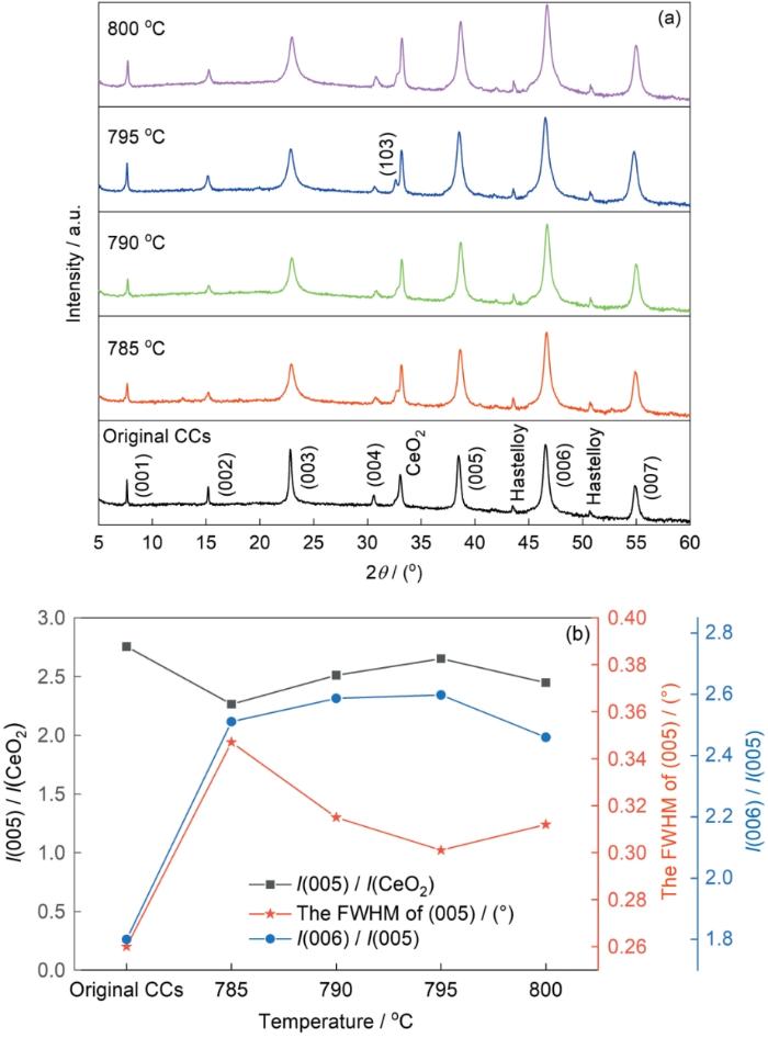
图2
在不同温度下在YGdBCO银带超导层制备的YBCO多晶膜的XRD谱以及(005)衍射峰的相对强度、半高宽和I(006)/I(005)峰强比
Fig.2
XRD patterns of YBCO polycrystalline films prepared on YGdBCO superconducting layers of the tapes at different temperatures (a), Relative intensity and full width at half maximum of (005) diffraction peak, and I(006)/I(005) (b)
图3给出了不同温度在YGdBCO银带超导层表面制备的多晶膜的表面形貌。如图所示,随着温度的升高YBCO非晶态前驱膜逐渐转化为多晶膜。在785 ℃生长的多晶膜表面的孔洞较多,晶粒生长不完全;在790 ℃生长的膜表面的孔洞尺寸明显减小,且晶粒间的连接性增强。在795 ℃生长的薄膜表面更加致密、晶粒生长较完全且分布均匀。而在800 ℃生长的膜表面出现较多裂纹和微孔,且多晶晶粒的结晶性降低。这表明,制备多晶膜的最优工艺是在795 ℃生长1 h。
图3
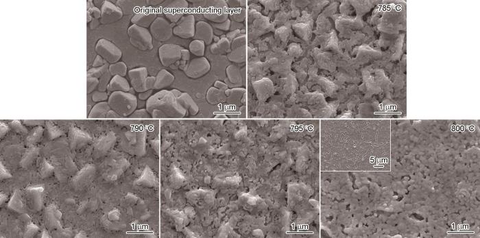
图3
原带超导层和在不同温度生长的YBCO多晶膜的SEM形貌
Fig.3
SEM morphology of the original superconducting layer and YBCO polycrystalline films prepared at different temperatures
用四引线法分别测试了原带材和沉积有多晶膜的带材在液氮温度、零场下的V-I特性。如图4所示,沉积多晶膜后的带材其Ic与原带材的相当。这表明,用此工艺在带材超导层上制备多晶膜不影响带材的电流传输特性。
图4
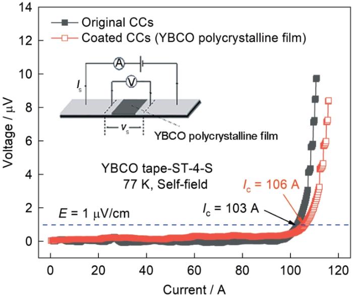
图4
原带材和沉积有YBCO多晶膜带材(795 ℃)的V-I曲线
Fig.4
V-I curves of the original tape and the tape deposited with YBCO polycrystalline film (795 oC)
2.2 YBCO多晶膜向单晶膜转化的最佳生长温度和时间
图5a给出了多晶膜在不同温度烧结30 min制备的单晶膜的XRD谱。可以看出,带材超导层在低氧压下高温热处理后,其(00l)单晶衍射峰的强度较高,表明带材超导层保持了较好的c轴织构。从图5b可见,随着烧结温度的提高(005)单晶衍射峰的强度均比多晶膜和原带的高,且在820 ℃达到最大值;(005)峰的半高宽均比多晶膜及原带的小,并在820 ℃达到最小值。同时,(103)多晶峰的强度随着温度的提高逐渐减小。上述结果表明,提高烧结温度可促进多晶晶粒向单晶晶粒转化,从而提高带材超导部分(包括母材YGdBCO超导层和YBCO超导焊料)的织构相比例。在低氧压环境下超过830 ℃的高温严重降低带材的结构和性能,因此转单晶温度的上限设定为820℃。
图5
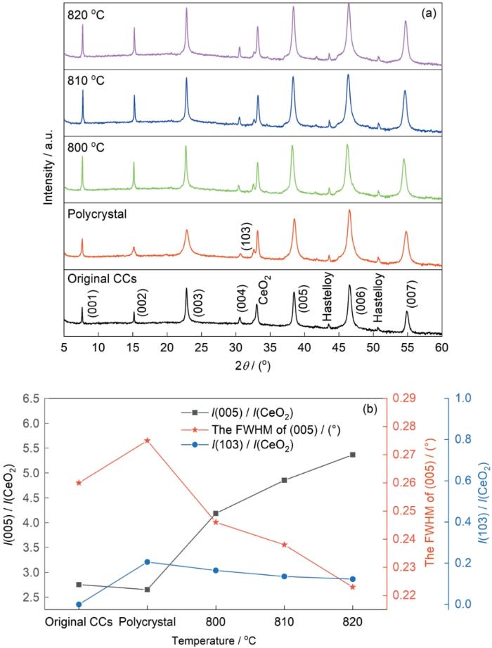
图5
YBCO多晶膜在不同温度生长的单晶膜的XRD谱以及(005)衍射峰相对强度与半高宽和(103)衍射峰相对强度
Fig.5
XRD patterns of YBCO single crystal films transformed from polycrystalline films at diff-erent temperatures (a), the relative intensity and full width at half maximum of (005) diffraction peak, and the relative intensity of (103) diff-raction peak (b)
图6
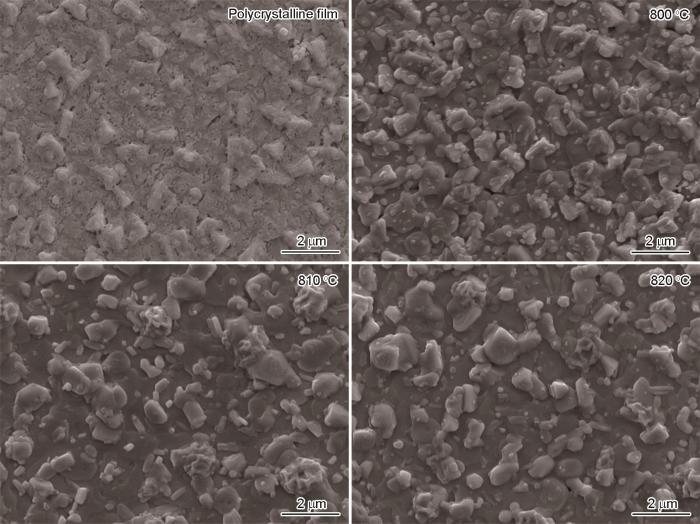
图6
YBCO多晶膜在不同温度生长的单晶膜的SEM形貌
Fig.6
SEM morphology of YBCO single crystal films transformed from polycrystalline films at different temperatures
图7给出了基于优化的转单晶温度,单晶生长时间对带材超导层的物相和织构的影响。从图7a可以看出,带材超导层在820 ℃和低氧压气氛中进行不同时间的热处理后,仍保持良好的c轴织构和较纯的超导相。图7b中不同时间制备的样品XRD谱中(005)衍射峰的强度都显著比原带和多晶膜的高,且随着烧结时间的延长而提高,烧结30 min时达到最大值;(005)峰的半高宽均显著比原带和多晶膜的低,且随着烧结时间的延长逐渐减小,烧结30 min时达到最小值。同时,(103)多晶峰的强度也随着烧结时间的延长逐渐降低。这表明,YBCO多晶膜在820 ℃低氧压气氛下烧结30 min使多晶晶粒充分转化为单晶晶粒,得到c轴织构最佳的单晶膜。
图7
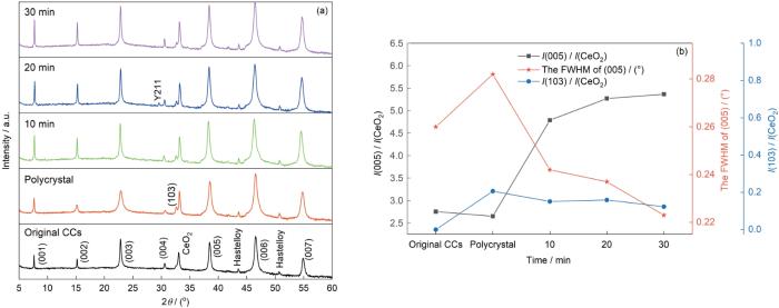
图7
多晶膜在820 ℃生长不同时间的单晶膜的XRD谱以及(005)衍射峰相对强度及其半高宽和(103)衍射峰相对强度
Fig.7
XRD patterns of single crystal films transformed from polycrystalline films at 820 oC with different time (a), the relative intensity and full width at half maximum of (005) diffraction peak, and the relative intensity of (103) diffraction peak (b)
图8给出了YBCO多晶膜在820 ℃生长不同时间的单晶膜的SEM形貌。可以看出,烧结不同时间的薄膜均具有典型的单晶外延生长形貌。随着烧结时间的延长薄膜表面的悬浮颗粒减少,表面的平整度提高,随机取向的多晶晶粒大多转化为(00l)取向的单晶晶粒。烧结30 min的样品,其表面更加平整致密。过长时间的高温烧结使带材的结构受到破坏和性能降低,不利于超导接头的制备,因此将转单晶的最大时长定为30 min。根据上述结果,单晶膜生长的优化热处理工艺是在820 ℃低氧压气氛下烧结30 min。
图8
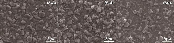
图8
YBCO多晶膜在820 ℃生长不同时间制备的单晶膜的SEM表面形貌
Fig.8
SEM surface morphology of single crystal films transformed from polycrystalline films at 820 oC with different growth time
图9
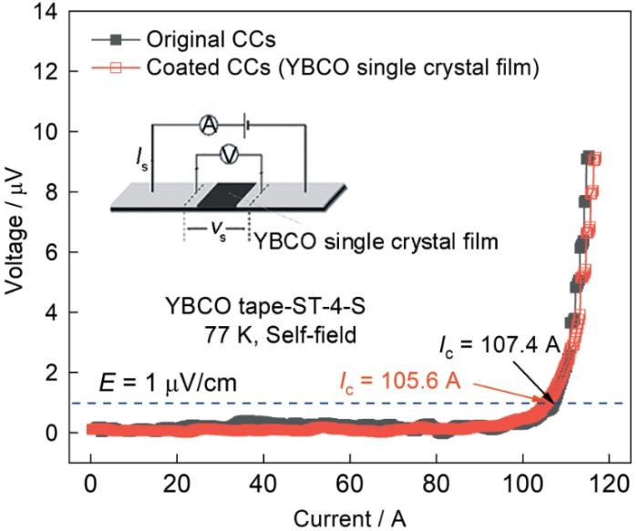
图9
YBCO多晶膜在820 ℃烧结30 min制备的单晶膜带材和原带材的V-I曲线
Fig.9
V-I curves of the original tape and the tape with single crystal film prepared by sintering YBCO polycrystalline film at 820 oC for 30 min
3 结论
将YBCO非晶前驱膜在795 ℃烧结1 h可制备出表面平整、晶粒均匀分布的YBCO多晶膜,将其在820 ℃烧结30 min可转化成具有较强c轴织构且表面悬浮颗粒较少、平整致密的单晶膜超导焊料。经历沉积多晶膜和多晶膜转化为单晶膜的热处理工艺的YGdBCO带材,在氧化退火后其临界电流Ic都与原带材相当,即超导焊料的生长不影响带材的超导电性。
参考文献
45.5-tesla direct-current magnetic field generated with a high-temperature superconducting magnet
[J].
World record 32.35 tesla direct-current magnetic field generated with an all-superconducting magnet
[J].
The electromagnetic properties of YGdBCO coated conductors with periodic micro-holes arrays
[J].
Development of research on new high temperature superconductors
[J].
Since discovered in 1911, the superconductors have evolved from single element, alloy to complex compounds with multiple elements.So far the proved highest superconducting transition temperature is 164 K (under pressure). In the long time of investigation on superconductivity, the understanding on the superconducting mechanism has been promoted significantly. The BCS theory which was greatly successful in describing the conventional superconductivity now is challenged by the new phenomena in some unconventional superconductors.Therefore the investigation of high temperature superconductivity mechanism is also at the dawn of major breakthrough. In this short overview, we will give a survey on the three families of high temperature superconductors, namely cuprates, iron based superconductors. Based on the experience accumulated in past decades, we propose some ideas in exploring high temperature superconductors.
新型高温超导材料研究进展
[J].超导自从1911年被发现以来, 研究对象经历了从简单金属, 到合金, 再到复杂化合物, 超导转变温度也逐渐提升, 目前已经提升到164 K(高压测量)。在研究新型高温超导材料的过程中, 对超导物理的理解也不断更新。在超导领域取得巨大成功的Bardeen-Cooper-Schrieffer理论, 似乎在一些新型的非常规超导体中不再适用, 因此非常规超导机理的理解也面临重大突破。本文将简单介绍目前发现的三类高温超导体: 铜氧化物超导体, 铁基超导体和二硼化镁超导体。结合目前研究中的一些经验, 对如何寻找新型超导体提出展望。
Design considerations and experimental results for MRI systems using HTS magnets
[J].
Critical current degradation and joint resistance rise of REBCO tape and coil during heat treatment
[J].
Analysis of a joint method between superconducting YBCO coated conductors
[J].
Lap joint resistance of YBCO coated conductors
[J].
Solderability study of RABiTS-based YBCO coated conductors
[J].
A superconducting joint for GdBa2-Cu3O7 - δ -coated conductors
[J].
A Superconducting joint for 2G HTS tapes
[J].
An efficient approach for superconducting joint of YBCO coated conductors
[J].
Superconducting joint of GdBa2Cu3O y coated conductors by crystallization of an additionally deposited precursor layer
[J].
Microstructures of superconducting joint between GdBa2Cu3O y -coated conductors via additionally deposited precursor films
[J].
Improving mechanical strength of YBCO bulk superconductors by addition of Ag
[J].
Superconducting joints for the 1.3 GHz persistent NMR magnet under JST-Mirai Program
[J].
Joint of REBa2Cu3O7 - δ coated conductors using metal organic deposition
[J].
Fabrication, microstructure and persistent current measurement of an intermediate grown superconducting (iGS) joint between REBCO-coated conductors
[J].
Towards a reliable bridge joint between REBCO coated conductors
[J].
Effects of chemical etching on structure and properties of Y0.5Gd0.5Ba2Cu3O7 - z coated conductors
[J].
