


1 实验方法
ZnO压敏陶瓷样品的制备:将分析级(摩尔分数)(95.185-x)%ZnO、1.05%Bi2O3、1%Co2O3、0.5%Cr2O3、1%Sb2O3、1.25%SiO2、0.015%Al、x%B(x=0.0, 1.5, 3.0, 4.5)与去离子水、分散剂和PVA (Polyvinyl alcohol)混合,然后加到球磨机中球磨4 h,得到均匀的混合浆液。在120℃用喷雾造粒设备将浆液制成粉末。将粉末压成直径为3 cm的圆盘,在400℃排胶48 h后置于1050℃马弗炉中烧结72 h。最后,将银浆喷涂在圆盘的上、下两面,在120℃烘箱中加热1.5 h制成电极。
用2410型数字源表在室温下测试电极的E-J (Electric field-current density)特性,用EMC Pro型冲击电流发生器测试残压比;将样品表面研磨、抛光并用丙酮清洗,用JSM-6700F型扫描电子显微镜观察其断面微结构;用Model H / max 2500型X射线衍射仪(XRD)分析结晶度;使用80型(Novocontrol,Winston-Salem)宽带电介质设备测量样品的C-V(Capacitance-voltage)特性曲线,频率为1 kHz;使用80型阻抗分析仪(Novocontrol)测试样品的复阻抗。
压敏陶瓷样品的非线性系数为
计算样品的势垒高度
2 结果和讨论
2.1 宏观电学性能
样品的电性能参数列于表1。从表1可以看出,当掺杂量为从0.0%增加到3.0%(摩尔百分数,下同)样品的泄漏电流从4.06 μA/cm2抑制到0.16 μA/cm2,非线性系数值从51增加至106。B掺杂对样品的击穿电压E1 mA和残余电压比K几乎没有影响。图1给出了不同B掺杂量样品的E-J图,可见E-J曲线的变化趋势与表1中的数据一致:从图1a可以看出,随着B掺杂量的增加样品的电压梯度E1 mA(0.1 μA/ cm2处的电场强度)没有明显的变化;在图1b的预击穿区中,随着B含量的增加拐点前的曲线越来越陡峭,拐点后的曲线越来越平坦,意味着样品非线性的改善[16]。压敏陶瓷的非线性系数α,主要由晶界处的势垒高度
表1 不同B掺杂量样品的电性能和微观结构参数
Table 1
B content /%, mole fraction | d / | Nd /1027m-3 | Ni /1018m-2 | /eV | Eb /V·mm-1 | JL /μA·cm-2 | α | K | Grain boundary resistance/kΩ |
|---|---|---|---|---|---|---|---|---|---|
| 0.0 | 6.58 | 1.86 | 1.81 | 1.66 | 470 | 4.06 | 51 | 1.57 | 29.69 |
| 1.5 | 6.61 | 1.98 | 2.03 | 1.98 | 474 | 2.52 | 67 | 1.58 | 45.14 |
| 3.0 | 6.62 | 2.59 | 2.86 | 2.98 | 475 | 0.16 | 106 | 1.57 | 74.68 |
| 4.5 | 6.66 | 2.23 | 2.27 | 2.17 | 479 | 0.25 | 86 | 1.59 | 52.53 |
图1
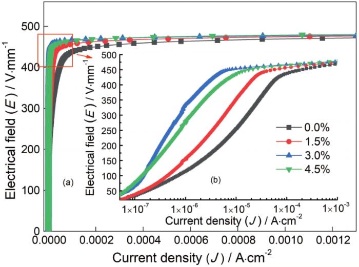
图1
不同B掺杂量样品的E-J图
Fig.1
E-J diagrams of samples with different B doping amounts: (a) E-J curve and (b) enlarged view at inflection point
2.2 微观电学性能
图2给出了不同B掺杂量样品的C-V特性曲线。根据C-V特性曲线的数据计算出样品的势垒高度
图2
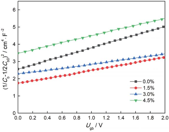
图2
不同B掺杂量样品的C-V曲线
Fig.2
C-V curves of samples with different B doping amounts (mole fraction)
2.3 微观结构和物相
图3
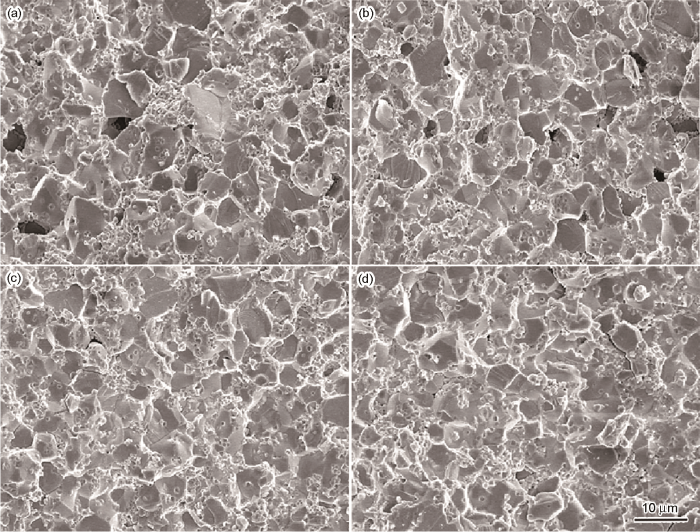
图3
不同B掺杂量样品的SEM照片
Fig.3
SEM images of samples with different B doping amounts (a) 0.0%, (b) 1.5%, (c) 3.0%, (d) 4.5%
图4

图4
典型样品的能量色散X射线光谱图像
Fig.4
Energy-dispersive X-ray spectral image of a typical sample: (a) measurement path and (b) element intensity
图5给出了不同B含量样品的相对密度和非线性的双y轴曲线图。随着B掺杂量从0.0%提高到3.0%样品的相对密度从75%提高到95%,与SEM图中样品气孔率的降低一致。相对密度的提高促进了样品整体电学性能的改善[21],与样品非线性和泄露电流的改善一致。图6给出了样品的X射线衍射谱。可以看出,样品的主要相为与较强峰对应的ZnO相,第二相有尖晶石相、Bi2O3相、焦绿石相、Bi-rich相和Zn3(BO3)2相。由于Al的掺杂量太小,没有检测到相关的衍射峰。B掺杂量为1.5%的样品Bi2O3相和焦绿石相消失,产生了新相Bi-rich相。继续提高B掺杂量到4.5%出现新相Zn3(BO3)2相,其反应方程式为
图5
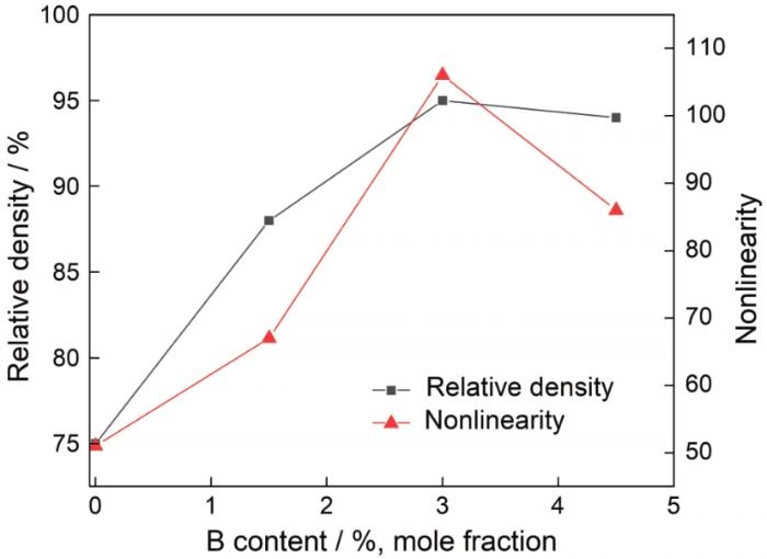
图5
不同B掺杂量样品的致密度-非线性折线图
Fig.5
Density-non-linear line graph of samples with different B doping levels
图6
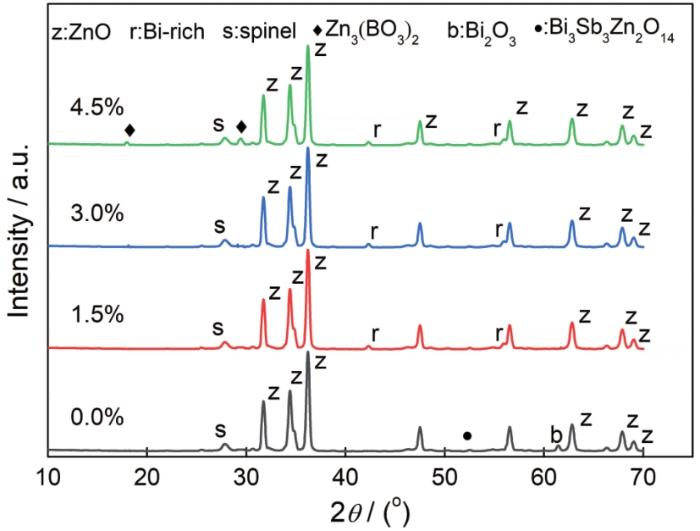
图6
不同B掺杂量样品的XRD衍射图
Fig.6
XRD diffraction patterns of samples with different B doping amounts
2.4 复阻抗特性
ZnO压敏陶瓷对低价位Al3+的存在非常敏感[22],这是掺杂Al产生很多副作用的原因。类似于钠离子的掺杂,部分Al3+溶解在铋的骨架中生成高电导率的连续富Bi液相,使泄露电流增大[23]。Al的掺杂也使样品的非线性恶化[13]。图7a给出了复阻抗测试的等效电路模型,其中Rgb与Cgb代表晶界阻抗,Rg代表晶粒电阻,对复数阻抗谱实验数据进行拟合,可计算出各样品的晶界电阻[24]。图7b给出了样品的阻抗半圆曲线,曲线与实轴右侧的交点代表样品的晶界电阻[25]。不同B掺杂量样品的晶界电阻,列于表1。可以看到,随着B含量从0.0%提高到3.0%样品的晶界电阻增大到74.68 kΩ,反映ZnO晶界稳定性的提高和对样品泄漏电流的抑制[26]。这解释了Al掺杂ZnO压敏陶瓷保持较低泄露电流的机制。B和Al的掺杂量分别为3.0%和0.015%的样品,在保持较低的残压比(1.57)的同时泄露电流和非线性性能也得到明显的改善。
图7
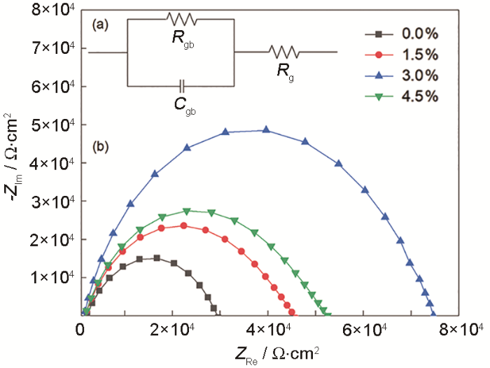
图7
B、Al共掺杂ZnO压敏陶瓷样品的阻抗等效电路图(a)和不同B掺杂量样品的复阻抗图像(b)
Fig.7
Impedance equivalent circuit diagram (a) and complex impedance image of samples with different B doping amounts (b)
3 结论
掺杂B能增大ZnO压敏陶瓷的晶界电阻,从而提高ZnO晶界的稳定性、抑制Al掺杂对ZnO压敏陶瓷电学性能的负面影响。B和Al共同掺杂,能在降低ZnO压敏陶瓷残余电压比的同时降低泄漏电流并改善样品的非线性。B、Al共掺杂ZnO压敏陶瓷最佳样品的非线性度高达106,残余电压比和漏电流分别低到1.57和0.16 μA/cm2,电压梯度为475 V/mm。
参考文献
The physics of metal oxide varistors
[J].
Advances in the synthesis of ZnO nanomaterials for varistor devices
[J]. J
The dc voltage dependence of semiconductor grain‐boundary resistance
[J].
Grain‐boundary interface electron traps in commercial zinc oxide varistors
[J].
High-temperature pyroelectricity of ZnO varistor ceramics
[J].
ZnO压敏陶瓷的高温热释电现象
[J].
Phase identification and electrical properties in ZnO-Glass varistors
[J].
The effects of heat treatment on B2O3-contained ZnO varistor
[J].
Effect of B2O3 doping on the microstructure and electrical properties of ZnO-based varistors
[J].
B2O3-doped ZnO-Pr6O11 based varistor ceramics
[J].
Boron and sodium co-doped ZnO varistor with high stability of pulse current surge
[J].
Low‐temperature sintering and electrical properties of BBSZ glass‐doped ZnO‐based multilayer varistors
[J].Appl
The effect of aluminium oxide on the residual voltage of ZnO varistors
[J].
The effect of aluminum on electrical properties of ZnO varistors
[J].
Effects of Fe and Al co-doping on the leakage current density and clamp voltage ratio of ZnO varistor
[J].
Influence of Bi2WO6 on electric properties of ZnO varistor ceramics
[J].
添加Bi2WO6对ZnO基压敏陶瓷电学性能的影响
[J].
Influence of SiO2 on electrical properties of the highly nonlinear ZnO-Bi2O3-MnO2 varistors
[J].
Influence of SiO2 on electrical properties of the highly nonlinear ZnO-Bi2O3-MnO2 varistors
[J].
Microstructure and electrical properties of Y2O3-doped ZnO-Pr6O11-based varistor ceramics
[J].
Low‐temperature sintering and electrical properties of BBSZ glass‐doped ZnO‐based multilayer varistors
[J].Appl
Effect of Cr2O3 addition on the microstructure and electrical properties of SnO2-based varistor
[J]. J
Sodium impurities in ZnO-Bi2O3-Sb2O3 based varistors
[J].
Improvement in nonlinear properties and electrical stability of ZnO varistors with B2O3 additives by nano-coating method
[J].
Conduction mechanism of non-Ohmic zinc oxide ceramics
[J].
Improvement in nonlinear properties and electrical stability of ZnO varistors with B2O3 additives by nano‐coating method
[J].
