



二硫化钼(MoS2)是一种典型的过渡金属硫化物,具有独特的层状结构、优异的电学、光学和机械性能[1,2],在光催化、能源存储、传感器等领域有广阔的应用前景[3,4]。用过渡金属元素改性,可提高MoS2二维薄膜材料的电-光、磁-电调控性能[5,6]。锰(Mn)是一种典型的过渡族金属元素,将其掺入MoS2二维薄膜能显著提高其磁性。Mishra等的第一性原理计算结果表明,Mn对Mo1-x Mn x S2二维薄膜磁矩的贡献约为1 µB[7]。Gao等还根据第一性原理计算了Mn掺杂对MoS2电子结构和磁性的影响,证实Mn的掺杂可引入局域磁矩,且Mn 3d轨道之间可通过Mo 4d和S 3p态耦合在Mn-S-Mn和Mn-S-Mo之间产生铁磁性交换作用,使材料的磁性提高[8]。Fan等发现, Mn掺杂的作用优于Fe、Co等元素,是因为Mn的原子半径与Mo更相近,掺杂对MoS2的结构影响较小[9]。Li等制备Mn掺杂MoS2纳米片并研究了其磁性与温度的关系[10]。本文制备一系列不同Mn掺杂浓度(x)的Mo1-x Mn x S2薄膜样品,系统研究Mn掺杂对MoS2薄膜磁性能的影响并阐述其物理机制,为研发掺杂MoS2二维薄膜器件提供实验依据。
1 实验方法
用化学气相沉积(CVD)法制备Mo1-x Mn x S2薄膜[11],主要步骤:实验用基片是尺寸为10 mm × 10 mm的单抛双面SiO2,先将硅基底依次用丙酮、酒精和去离子水超声清洗,然后在氮气气流中干燥。将清洗后的基片置于CVD生长炉中,在炉中放入硫源(S粉)(AR 99.5%,Sigma-Aldrich)、钼源(MoO3)(AR 99.5%,Aladdin)和锰源(MnO2) (AR 99%,Damas),温度区分为两个。将S粉的区域加热至150 ℃,将反应物区域(MoO3和MnO2)加热至750 ℃,升温速率为25 ℃/min。在生长过程中向炉中通入流量为1.8 m3/h的氩气。加热至反应温度保温15 min后即可在硅基衬底上生长出Mn掺杂的Mo1-x Mn x S2薄膜。薄膜的CVD生长示意图在图1中给出。为了研究Mn掺杂浓度(x)对Mo1-x Mn x S2薄膜性能的影响,调节反应物中钼源和锰源的投料比制备出一系列不同Mn掺杂浓度的Mo1-x Mn x S2薄膜样品。然后测试薄膜的微结构和磁性能[12,13]。
图1

图1
薄膜的CVD生长装置示意图
Fig.1
Schematic diagram of the CVD growth device for thin films
用光学显微镜(BX51/BX52)和原子力显微镜(AFM, Multimode 8-HR)测试薄膜的表面光学结构和表面形貌。用X射线衍射仪(XRD, Bruker D8 Advance)测量薄膜的XRD谱。用Raman光谱分析仪(Horiba LabRAM HR Evolution)测试薄膜的Raman散射光谱。用X射线光电子能谱仪(XPS, monochromatic Al Kα X-rays,Kratos Axis Supra TM system, hv= 1486.69 eV)测量薄膜的X射线光电子能谱,确定薄膜表面元素的结合能、元素组成和化学状态。用综合物性测量系统(PPMS, dynacool-9)测量薄膜的磁化强度和矫顽力等磁性能。
2 结果和讨论
2.1 薄膜的晶体结构和成分
图2给出了Mo1-x Mn x S2薄膜表面的光学照片,可见其由边长为40~60 μm的不同三角形结构组成,结晶度较好。磁性测试前,用划片机在10 mm × 10 mm大面积薄膜上切割出S = 5 mm × 5 mm的样片供PPMS测试,用AFM测量不同掺杂薄膜的厚度h,插图给出了薄膜的AFM图像和薄膜厚度的轮廓测试曲线,薄膜的厚度约为60 nm。薄膜的体积约为V =S × h。
图2

图2
Mo1-x Mn x S2的光学照片,插图给出了AFM测试的薄膜厚度
Fig.2
Optical photograph of Mo1-x Mn x S2, inset shows the film thickness as tested by AFM
前驱体的浓度比与实验合成的Mo1-x Mn x S2薄膜中的Mn和Mo的比值略有不同,用XPS测试了薄膜中元素的占比,以此定量标注Mo1-x Mn x S2薄膜中Mn的掺杂浓度x。表1列出了不同浓度样品的投料比与XPS测试的元素占比数据。
表1 不同样品的投料比和XPS测试的元素占比数据
Table 1
| Number | Sulfur powder / mg | MoO3/MnO2 powder / mg | x in Mo1-x Mn x S2 by calculation | x in Mo1-x Mn x S2 measured by XPS |
|---|---|---|---|---|
| A1 | 200 | 20/0 | 0 | 0 |
| A2 | 200 | 18/2 | 0.073 | 0.034 |
| A3 | 200 | 17/3 | 0.112 | 0.048 |
| A4 | 200 | 16/4 | 0.151 | 0.079 |
| A5 | 200 | 15/5 | 0.192 | 0.097 |
| A6 | 200 | 14/6 | 0.234 | 0.127 |
| A7 | 200 | 12/8 | 0.322 | 0.131 |
| A8 | 200 | 10/10 | 0.416 | 0.221 |
图3给出了MoS2和Mo1-x Mn x S2薄膜样品的XRD谱,谱中2θ = 69.21°处的衍射峰属于基底SiO2中Si的(400)晶面,2θ = 14.59°、32.98°和60.48°处的3个衍射峰分别对应六边形结构的MoS2的(002)、(100)和(112)晶面(JCPDS No. 37-1492)[14,15],表明薄膜中存在MoS2相和结晶度较好。在Mo1-x Mn x S2薄膜的衍射谱中,在2θ = 14.55°、33.07°和60.25°处的3个衍射峰与MoS2的(002)、(100)和(112)晶面相对应,在2θ = 44.33°处的新衍射峰与MnS2相的(220)晶面(JCPDS No. 25-0549)一致[16]。可以观察到,随着掺杂浓度x的增大MnS2相(220)的衍射峰强度提高,也印证了Mn元素在Mo1-x Mn x S2薄膜中掺杂浓度的提高。这表明,Mn已经掺入MoS2薄膜中。
图3

图4给出了Mo1-x Mn x S2薄膜的Raman光谱曲线,可见谱中出现了波数约为385和406 cm-1两个主要振动峰,分别对应面内振动E
图4

图4
不同Mn掺杂浓度Mo1-x Mn x S2薄膜的Raman光谱
Fig.4
Raman spectra of Mo1-x Mn x S2 films with different Mn doping amount
在本文的实验中,Mn原子半径为0.139 nm,Mo原子半径为0.145 nm,较为接近。因此,掺杂后薄膜晶格的整体结构没有太大的变化,没有引入较大的外加应力,因此E
图5给出了XPS测试的Mo、S和Mn的核心能级光谱。图5a的全谱图表明,样品中有掺杂的Mn以及MoS2基体中的主要元素成分Mo和S。图5b表明,Mo 3d的两个主要峰位分别出现在227.7 eV (Mo 3d5/2)和231.0 eV (Mo 3d3/2)处,进行解卷积将Mo 3d5/2和Mo 3d3/2分解为两个组分,以进行良好的拟合。第一组分位于227.5和230.7 eV,对应化学计量比的本征MoS2,反映完整的Mo-S键合特性。第二组分位于227.9 eV和231.3 eV处,结合能比化学计量MoS2略低(约0.4 eV),对应具有硫空位的缺陷或亚化学计量MoS2。Mo的半峰全宽(FWHM)约为1.12 eV,表明样品中的二硫化钼具有良好的化学计量特性和晶体完整性[19]。
图5

图5
Mo1-x Mn x S2的XPS谱
Fig.5
XPS spectra of Mo1-x Mn x S2 (a) full spectrum, (b) Mo 3d, (c) S 2p, (d) Mn 2p
图5c给出了S元素的XPS谱。S 2p谱的结合能位置和峰的分裂(S 2p3/2和S 2p1/2)表明,S元素主要以化学计量的S2-状态存在,样品Mo1-x Mn x S2的化学计量比良好。在样品的谱中未出现明显的硫缺陷峰或其他化学状态的硫峰,表明硫空位的浓度较低,进一步确认了S元素的化学价态与化学计量MoS2的特性一致[20]。图5d表明,Mn 2p的XPS谱由一个位于结合能为640.2 eV和652.2 eV的突出双峰组成,并分别伴随着一个分别位于644.9 eV和656.7 eV的卫星双峰。其原因是,在MnO2原料的加热过程中,随着氧气的释放生成了三种低价锰氧化物。不同氧化态的锰呈现出不同的化学环境,从而产生不同的电子结构和XPS结合能。
以上一系列的元素表征和分析,都证实Mn原子已经掺入MoS2中。
2.2 薄膜的磁性能
图6给出了不同Mn掺杂浓度的Mo1-x Mn x S2薄膜的低温(2 K)磁滞回线。插图中MoS2的磁化曲线表明,MoS2具有典型的反铁磁性。但是,掺杂后的Mo1-x Mn x S2薄膜出现磁滞回线,表现出典型的铁磁行为,并且饱和磁化强度和矫顽力也随着Mn掺杂程度的不同而变化。Mishra等和Gao等基于不同Mn掺杂浓度的模型进行了第一性原理计算[7,8],发现Mn替代Mo使Mn未成对的3d电子在自旋向上/向下通道上发生分裂,增强了自旋极化和局域磁矩,使低Mn掺杂浓度的薄膜具有铁磁性。随着Mn掺杂浓度的提高Mn 3d轨道之间通过Mo 4d和S 3p态耦合在Mn-S-Mn和Mn-S-Mo之间产生交换作用。按照Goodenough-Kanamori规则[21],如果两个阳离子与阴离子共线呈180°,则两个阳离子之间的相互作用为反铁磁性;如果两个阳离子与阴离子介入导致超交换作用呈90°夹角,其相互作用为铁磁性。因此,因Mn掺杂浓度的不同体系中同时存在铁磁耦合和反铁磁耦合两种机制。
图6
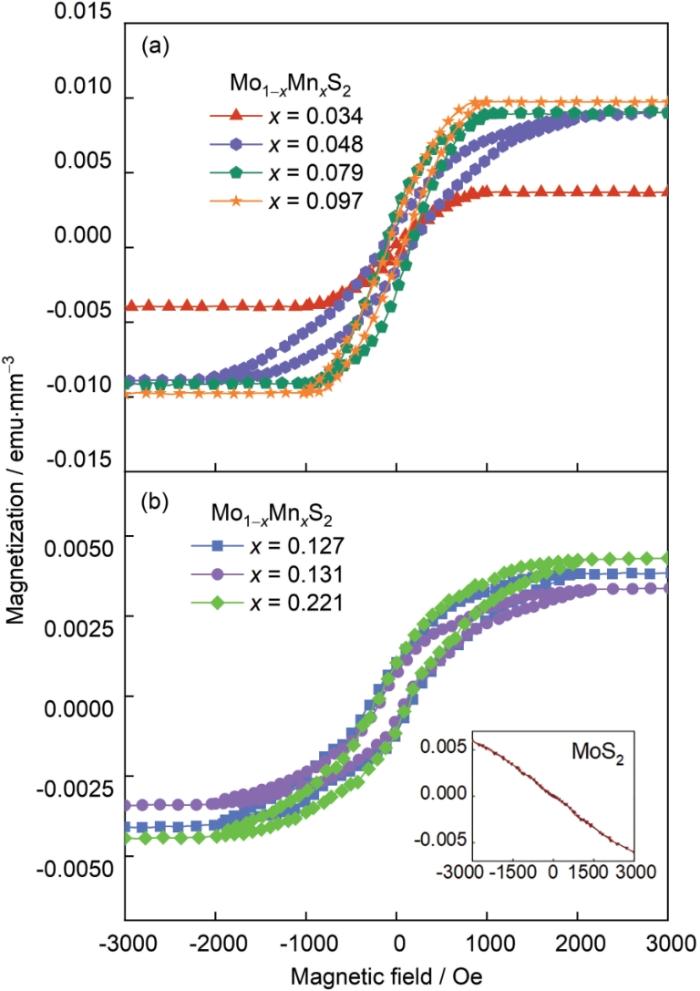
图6
在2 K温度下不同Mn掺杂浓度样品的磁滞回线,插图给出了MoS2的磁性测量曲线
Fig.6
Hysteresis of samples with different Mn doping amout (a) x = 0.034、0.048、0.079、0.097, (b) x = 0.127、0.131、0.221 at 2 K, the inset of (b) shows the magnetic properties of MoS2 film
进一步分析Mo1-x Mn x S2薄膜的磁性能,得到了薄膜样品的饱和磁化强度Ms和矫顽力Hc与Mn掺杂浓度x的关系(图7)。从图7可见,饱和磁化强度Ms先上升后下降。掺杂浓度约为9.7%的薄膜,其饱和磁化强度达到了最大值0.0096 emu/mm3,比少量掺杂的薄膜提高了2~3倍。体系中的局域磁矩,使低Mn掺杂浓度的薄膜具有铁磁性。随着Mn掺杂浓度的提高,Mn-S-Mn和Mn-S-Mo之间产生铁磁交换作用。一定浓度的Mn掺杂,使体系的铁磁性增强。随着Mn掺杂浓度的提高薄膜晶格的局部扭曲使反铁磁性交换作用增强,两种交换作用机制的竞争降低了体系的铁磁性。实验中,低Mn浓度(x <5%)的薄膜,较低的Mn离子浓度使磁性交换通道较少,其磁性主要源于Mn离子提供的局域磁矩,因此饱和磁化强度Ms随之降低。在中Mn浓度(x ≈ 5%~10%)的薄膜中,进入晶格的Mn离子较多而提高了铁磁交换作用,Ms随x的增大而很快提高且在x~9.7%达到最大。随着Mn掺杂浓度进一步提高(x >10%)薄膜晶体的局部扭曲使不同邻近的Mn-S-Mn和Mn-S-Mo路径的键角分布改变,有些键角偏向铁磁性的90°,有些偏向反铁磁性的180°,两种耦合相互竞争削弱了薄膜整体的铁磁性,使Ms不再升高且有所下降。同时,从图7可见,Mo1-x Mn x S2薄膜的矫顽力随着Mn掺杂浓度的提高而增大。其原因是,Mn掺杂引起的钉扎效应阻碍了畴壁移动,进而使得薄膜的矫顽力随之增大。因此,控制Mn的掺杂量可调控Mo1-x Mn x S2薄膜的磁性能。
图7

图7
饱和磁化强度和矫顽力的变化与Mn掺杂浓度的关系
Fig.7
Variation of saturation magnetization strength and coercivity with variation of Mn doping amount
将饱和磁化强度Ms (emu/mm3)的实验值与根据第一性原理计算出的理论值比较,即以玻尔磁子表示的每个Mn原子的磁矩m'(μB/Mn atom, μB为玻尔磁子)。根据Mo0.952Mn0.048S2计算出其每个Mn原子的磁矩。样品Mo0.952Mn0.048S2的饱和磁化强度的测试值为Ms = 0.00866 emu/mm3,显微镜和台阶仪测试得薄膜体积为V = 0.0013 mm3,则总磁矩m为Ms × V = 1.13 × 10⁻⁵ emu。已知1个玻尔磁子1 μB ≈ 9.274 × 10⁻²¹ emu,所以总磁矩m(μB)为1.21 × 10¹⁵ μB。化学计量比为Mo0.952Mn0.048S2表示每个化学式中有0.048个Mn原子,摩尔质量为158.17 g/mol,根据MoS2的密度ρ ≈ 5.06 g/cm3 [22],可得摩尔数为4.16 × 10⁻⁸ mol,相应样品中Mn原子数NMn为1.20 × 10¹⁵个。最终得每个Mn原子的磁矩为1.21 × 10¹⁵ μB/1.20 × 1015 = 1.01 μB。即掺杂的Mn原子浓度为4.8%的样品,每个Mn原子的磁矩为1.01 μB,与第一性原理计算的理论计算值1 μB一致[7]。这表明,实验的掺杂效果和Mo1-x Mn x S2薄膜的磁性能较好。实验结果证实,Mn的掺杂可在MoS2晶体中引入额外的磁矩,使磁交换相互作用增强而显著提高薄膜材料的磁性能。
3 结论
用化学气相沉积法可制备不同Mn掺杂浓度的Mo1-x Mn x S2薄膜。Mn元素掺入MoS2薄膜可增强MoS2薄膜的磁性能。MoS2薄膜磁性的增强,主要源于Mn原子引入的局域磁矩以及增强的磁交换相互作用,揭示了Mn掺杂对二维材料磁性能调控的物理机制,明确了Mo1-x Mn x S2薄膜磁性能与Mn掺杂浓度之间的定量关系。
参考文献
Single-layer MoS2 transistors
[J].
Two-dimensional materials are attractive for use in next-generation nanoelectronic devices because, compared to one-dimensional materials, it is relatively easy to fabricate complex structures from them. The most widely studied two-dimensional material is graphene, both because of its rich physics and its high mobility. However, pristine graphene does not have a bandgap, a property that is essential for many applications, including transistors. Engineering a graphene bandgap increases fabrication complexity and either reduces mobilities to the level of strained silicon films or requires high voltages. Although single layers of MoS(2) have a large intrinsic bandgap of 1.8 eV (ref. 16), previously reported mobilities in the 0.5-3 cm(2) V(-1) s(-1) range are too low for practical devices. Here, we use a halfnium oxide gate dielectric to demonstrate a room-temperature single-layer MoS(2) mobility of at least 200 cm(2) V(-1) s(-1), similar to that of graphene nanoribbons, and demonstrate transistors with room-temperature current on/off ratios of 1 × 10(8) and ultralow standby power dissipation. Because monolayer MoS(2) has a direct bandgap, it can be used to construct interband tunnel FETs, which offer lower power consumption than classical transistors. Monolayer MoS(2) could also complement graphene in applications that require thin transparent semiconductors, such as optoelectronics and energy harvesting.
In-situ growth of MoS2 on the surface of polyquinazoline conjugated microporous polymers and its electrocatalysis hydrogen performance
[J].
原位生长在聚喹唑啉基共轭微孔聚合物表面的MoS2及其析氢性能
[J].合成一种三环喹唑啉的共轭微孔聚合物(TQ-CMPs)并用水热法使二硫化钼原位生长在其骨架表面,制备出一种新型复合电催化析氢催化剂并研究了它的电催化析氢活性。结果表明,TQ-CMPs与MoS<sub>2</sub>的质量比为2∶1的催化剂具有优异的电催化析氢活性,其过电势为71 mV,Tafel斜率为52 mV·dec<sup>-1</sup>。比表面积较大的TQ-CMPs,使MoS<sub>2</sub>的分散度提高、避免了MoS<sub>2</sub>的堆积和聚集并使更多的MoS<sub>2</sub>边缘暴露,从而提高了催化剂的效率。TQ-CMPs丰富的孔道结构和延伸的π共轭骨架,有利于质量运输和电荷转移。
High frequency permittivity of rare-earth Er-doped MoS2 films
[J].
Study on photoelectric properties of manganese-doped MoS2 thin films
[J].
Interlayer-incorporation of MoS2 (TM-MoS2) to achieve unique magnetic and electronic properties for spintronics
[J].
Anti-oxidization and electronic properties of Ti doped MoS2 films
[J].
Ti掺杂MoS2薄膜的抗氧化性和电学性能
[J].用磁控溅射在硅片上制备MoS<sub>2</sub>和Ti-MoS<sub>2</sub>薄膜,并将其在恒温恒湿箱中在AT 30℃、RH 70%条件下存储360 h。使用XRD谱、XPS谱和紫外-可见分光光度计、四探针测试仪表征分析薄膜的结构、在恒温恒湿条件下存储前后的表面化学状态和电学性能,研究了Ti掺杂对薄膜抗氧化性和电学性能的影响。结果表明:Ti掺杂影响MoS<sub>2</sub>薄膜的晶体取向。随着Ti靶电流的增大薄膜的结晶性变差,Ti靶电流为0.6A时薄膜呈无定型结构且禁带宽度减小、电导率提高;在恒温恒湿条件下存储后薄膜的部分氧化而呈MoS<sub>2</sub>与MoO<sub>3</sub>的复合状态,随着Ti靶电流的增大I<sub>Mo-O</sub>/I<sub>Mo-S</sub>比提高、禁带宽度略有增大,Ti靶电流为0.4A的Ti-MoS<sub>2</sub>薄膜其化学稳定性较高。
Impact of Mn- and Fe-doping on electronic and magnetic properties of MoX2 (X = S, Se) monolayer
[J].
Magnetic properties of Mn-doped monolayer MoS2
[J].
Ferromagnetism in transitional metal-doped MoS2 monolayer
[J].
Room-temperature ferromagnetism in layered Mn-substituted MoS2
[J].
Manganese doping of monolayer MoS2: the substrate is critical
[J].Substitutional doping of transition metal dichalcogenides (TMDs) may provide routes to achieving tunable p-n junctions, bandgaps, chemical sensitivity, and magnetism in these materials. In this study, we demonstrate in situ doping of monolayer molybdenum disulfide (MoS2) with manganese (Mn) via vapor phase deposition techniques. Successful incorporation of Mn in MoS2 leads to modifications of the band structure as evidenced by photoluminescence and X-ray photoelectron spectroscopy, but this is heavily dependent on the choice of substrate. We show that inert substrates (i.e., graphene) permit the incorporation of several percent Mn in MoS2, while substrates with reactive surface terminations (i.e., SiO2 and sapphire) preclude Mn incorporation and merely lead to defective MoS2. The results presented here demonstrate that tailoring the substrate surface could be the most significant factor in substitutional doping of TMDs with non-TMD elements.
Substrate-induced strain and charge doping in CVD-grown monolayer MoS2
[J].Due to its electronic-grade quality and potential for scalability, two-dimensional (2D) MoS2 synthesized by chemical vapor deposition (CVD) has been widely explored for electronic/optoelectronic applications. As 2D MoS2 can be considered a 100% surface, its unique intrinsic properties are inevitably altered by the substrate upon which it is grown. However, systematic studies of substrate-layer interactions in CVD-grown MoS2 are lacking. In this study, we have analyzed built-in strain and charge doping using Raman and photoluminescence spectroscopy in 2D MoS2 grown by CVD on four unique substrates: SiO2/Si, sapphire, Muscovite mica, and hexagonal boron nitride. We observed decreasing strain and charge doping in grown MoS2 as the substrates become less rough and more chemically inert. The possible origin of strain was investigated through atomic force microscopy roughness measurements of the as-grown layer and substrate. Our results provide direction for device optimization through careful selection of the growth substrate and pave the way for further investigations to unravel the complex nature of the 2D monolayer-substrate interface.
Layer-controlled CVD growth of large-area two-dimensional MoS2 films
[J].
Random stacking in MoS2- x sputtered thin films
[J].
Synergy between nanozymes and natural enzymes on the hybrid MoS2 nanosheets/graphite microfiber for enhanced voltammetric determination of hydrogen peroxide
[J].A biosensor for hydrogen peroxide (HO) has been developed based on the use of MoS nanosheets and graphite that are assembled to form a microfiber hybrid structure. The MoS nanosheets are synthesized in situ on a graphite microfiber. The chemical composition and surface morphology of the microfiber hybrid structure has been characterized. The microfiber is shown to display peroxidase-mimicking activity. In the next step, horseradish peroxidase, methylene blue, and chitosan are co-immobilized on the microfiber electrode. The use of MoS nanosheets warrants high electrochemical activity of immobilized enzyme on the electrode surface. The modified microfiber electrode, best operated at a voltage of - 0.3 V (vs. Ag/AgCl), can be used to sense HO with a linear response in the 0.1 to 90 μM concentration range and with a determination limit of 30 nM (at S/N = 3). The good response is attributed to the synergistic enhancement of the synthetic nanozymes (few-layered MoS nanosheets) and immobilized natural horseradish peroxidase (HRP). Grapical abstract.
Synthesis and characterization of ZnS quantum dots on MnS2 nanoparticles for photo-assisted electrochemical degradation of drug compound
[J].Herein, ZnS quantum dots on MnS2 (ZnS/MnS2) nanoparticles. Was prepared via the facile and simple method. The ZnS/MnS2 nanocomposites were characterized into attained optical, morphological, structural, and surface attributes using different analytical routs. The average crystallite size of MnS2 and ZnS/MnS2 nanocomposites are 27.2 and 14.8nm via calculated from Scherrer's equation. Subsequent, the photo-catalytic and -electrochemical attributes of synthesized ZnS/MnS2 nanocomposites were as well as presented. The ZnS/MnS2 nanocomposites electrode represented a potential influence on the decomposition of acetaminophen, which was higher than that of MnS2 nanoparticles electrode. The high amount of ZnS QDs in MnS2 samples has a high decomposition efficiency of acetaminophen due to the conduction band position and valence band position of ZnS QDs are higher than that of MnS2. Influencing major factors on the decomposition of acetaminophen were evaluated and the removal of acetaminophen was performed at pH:3, 60mA cm(-2), and 0.1M NaCl concentration. The prepared electrode represented great stability and indicated the highest possible for treatment technology of wastewater. Comparison of the performances of the photo-assisted electrochemical (PAEC) electrochemical (EC) and photo-catalytic indicated that the hybrid process (PAEC) has high efficiency for acetaminophen degradation.
In situ monitoring of the thermal-annealing effect in a monolayer of MoS2
[J].
Symmetry-dependent phonon renormalization in monolayer MoS2 transistor
[J].
Synthesis and characterization of monolayer Er-doped MoS2 films by chemical vapor deposition
[J].
Controlled argon beam-induced desulfurization of monolayer molybdenum disulfide
[J].


