



具有超导电性、光电效应[4~6]或多铁效应[7,8]的二维材料[1~3],可用于制造新一代光电器件[9]。WSe2的空穴迁移率优异[10,11]且光吸收系数较大[12],可用于制造光电探测器[13]和太阳能电池[14]。基于WSe2/Q2DEG的van der Waals异质结具有可充电的光电导(Chargeable photoconductivity, CPC)效应[15,16]。这类器件的CPC效应源于异质结界面空间电荷区(Intrinsic space charge region, ISCR)内长寿命光生载流子的存储,其中WSe2区域的光生空穴起主导作用。受到激光照射时,ISCR区域中的光生载流子同步生成和存储;撤去光照并施加偏置电压后存储的载流子高效复合,从而使光电流显著增强。提高偏置电压可扩展载流子复合的深度,使更多深能级的光生载流子参与导电,从而进一步提高光电流强度。
以铋铁氧体(BiFeO3, BFO)[17~20]为代表的室温多铁材料[21],兼具铁电性和反铁磁性[22~24]。BFO自发极化场可调控载流子的分离和输运,其极化电场使相邻的半导体层能带弯曲而形成微米级扩展耗尽区,能抑制载流子的复合[25,26]和延长其寿命。虽然对BFO材料光电性能的研究取得了一定的进展,但是关于其与二维材料的集成[27~29],特别是将薄膜集成在二维的van der Waals异质结上的研究较少。鉴于此,本文提出一种具有光存储功能基于多铁调控的新型异质结架构。先将BFO薄膜脉冲激光沉积(Pulsed laser deposition, PLD)在SrTiO3 (STO, (001)取向)衬底作为器件的掩埋层,然后用Ar+离子轰击辅助(Ar+-ion-bombardment assistant, AIBA)制备n型准二维电子气(Q2DEG)电极,最后转移p型WSe2制备出WSe2/BiFeO3/Q2DEG混合异质结并研究其光电性能。
1 实验方法
器件的制备:将PLD和AIBA相结合在单晶STO,(001)取向衬底上制备WSe2/BFO/Q2DEG混合异质结。先在750 ℃和13 Pa氧压条件下在STO衬底上制备厚度约为约40 nm的BFO外延薄膜。激光频率为3 Hz,激光功率为1.5 J/cm2。然后将几层WSe2纳米片从其块状晶体上剥离并转移到BFO薄膜表面。最后,在表面光刻出所需的电极图案,并进行磁控溅射和AIBA分别在混合异质结的两端沉积不同的电极。直流溅射90 s (功率为80 W)在WSe2纳米片上沉积出金(Au)电极。然后,在250 V加速电压作用下用Ar+离子轰击样品表面10 min,制备出高导电性的Q2DEG电极。
性能表征:用X射线衍射仪(XRD)测试BFO薄膜样品的XRD谱,2θ的范围为20°~80°。用Raman光谱仪(Horiba,LabRAM HR Evolution, 532 nm光源)测试二维材料WSe2的Raman光谱,测量范围为160~300 cm-1。用光学显微镜(BX51/BX52)和原子力显微镜(AFM)观测器件的光学结构和表面形貌。用压电力显微镜(PFM)测定BFO薄膜的铁电特性(I-V曲线和光电性能)。照射光源为可调功率激光器,波长范围为405~808 nm,用光纤束将激光传输至样品室,样品放置在综合物性测量系统中(PPMS),测试温度为2~300 K,磁场为0~9 T。导电探针对BFO薄膜施加了范围为-6 V至6 V的面外电压,测试了BFO薄膜的PFM结果。
2 结果和讨论
图1a给出了WSe2/BFO/Q2DEG横向混合异质结的结构示意图,可见其由垂直堆叠的BFO单晶薄膜和WSe2二维层状纳米片组成,两端的电极由Au电极和右侧离子轰击形成的Q2DEG电极组成。由图1b可见在光学显微镜下器件结构的形态特征,Au/WSe2与Q2DEG/WSe2之间有两个界面。图1c给出了器件的AFM形貌结构,可见其表面的微观结构特征。高度轮廓的测量结果表明,这种器件有清晰的三层递进台阶,与图1b所示结果一致。离子轰击深度约为80 nm,薄膜的厚度约为40 nm。图1d给出了BFO薄膜样品的XRD谱,可见STO衬底(00l, l = 1, 2, 3)和BFO薄膜(00l, l = 1, 2, 3)的尖锐特征峰。这表明,已经成功地制备出单晶外延薄膜。从图1e可见封闭的蝴蝶形图样,表明BFO薄膜实现了良好的极化翻转,即其具有优异的铁电特性。图1f给出的Raman光谱,验证了在器件的制备过程中WSe2纳米片的完整性。分别在249 cm-1和259 cm-1处观察到了
图1

图1
器件的形貌和结构
Fig.1
Morphology and characterization of the device (a) structural schematic diagram, (b) optical microscope image and (c) AFM surface topography mapping of heterojunction device, the inset is a step height curve, (d) XRD θ-2θ scan of the BFO film, (e) the amplitude and phase hysteresis loops of the BFO films, (f) raman spectrum of the WSe2 flake in the heterojunction
图2a给出了在单次充电(光照时间为30 s)后,连续施加正偏压(1~16 V)的电流-电压(I-V)特性回线。可以看出,施加1~4 V的正偏压时器件没有产生光电流,偏压达到5 V时产生了显著的光电流。同时,随着正偏压的增大,光电流随之增大。其原因是,低电压区存储的光生载流子耗尽后,更高的偏压使储存在更深界面态复合中心中的长寿命光生载流子跨越内建势垒,从而提高了光生电流的输出。在20 K的温度下用405 nm的光照充满电后,调节偏置电压的步长(Vr)测量了光生载流子释放过程的I-V特性(图2b)。可以看出,随着Vr的提高光电流增大,不同于线性增加的常规光电导效应。器件处于充满电的状态时,其存储电荷量固定。根据CPC效应,随着Vr的提高光生载流子释放速率随之提高,使光电流显著增大。图2c给出了405 nm的单次光照充满电后连续测得的5次I-V回线,可见在第一次循环中消耗了大部分光生载流子。但是,仍有少量残留的电荷被捕获在空间的电荷区内,阻碍器件返回到本征绝缘状态。为了研究CPC效应产生的光电流和常规光电导效应产生的电流,对比了在10 V偏压下光照充电和持续光照的电流(图2d)。可以看出,器件充电后在黑暗中测得的放电电流明显高于持续光照下的电流。其原因是,无偏压时光照产生的光生载流子复合受到抑制而持续累积,从而在暗态下释放出更大的电流。相反,在同时施加偏压和光照的条件下(即持续光照状态),光生载流子更倾向于快速复合而非累积,从而使产生的光生电流比CPC效应产生的电流小一个量级。在实验结果的基础上,本文建立一个理论模型解释CPC效应。图2e中的左右两侧为Q2DEG和WSe2,分别为pn结的n区和p区。上半部分为光充电过程,下半部分为放电过程。示意图表明,CPC效应源自内在ISCR中存在的无限寿命的光生载流子。为了说明光生载流子的生成和存储,用半径为0.7 µm激光束照射异质结的不同位置。结果表明,存储在ISCR中的光生载流子是WSe2区域的光生空穴(Photogenerated holes, PGHs)。PGHs填充ISCR,形成了光生载流子和BFO的铁电极化场诱导WSe2能带发生微米尺度的弯曲形成PGHs存储区域。这三个区域确定了器件的电子传输,即n区域、p区域和PGHs存储区域。在光充电期间,Ar+离子轰击工艺引入的缺陷在WSe2/Q2DEG界面形成了高密度的深能级陷阱态。这些界面态成为高效的载流子复合中心,能捕获并长期束缚PGHs。其结果是,界面附近的区域优先由PGHs填充,然后逐渐填充ISCR中的其他区域。在暗态放电过程中,偏置电压局部调制界面的能带结构,降低被捕获空穴所处的势垒高度而使存储在ISCR中的PGHs释放。这表明,该器件的CPC效应主要源于异质结内部ISCR中存储的无限长寿命光生载流子,主要是存储在WSe2区域的PGHs。激光照射在全部ISCR内同步产生存储光生载流子。关闭激光施加外加偏置电压,使存储的光生载流子高效复合,从而释放出极大的光电流。
图2

图2
器件的CPC效应测试
Fig.2
CPC effect of the device at a temperature of 20 K (a) the I-V curves of the device measured under various maximum positive forward bias voltages (1-16 V) after a single full charging process, (b) dependence of photocurrent on Vr after full charging, (c) continuously measured I-V loops after a single full charging under a 405 nm illumination,(d) I-V loops measured under continuous illumination and single charging, (e) schematic diagram of CPC effect
图3

图3
器件CPC效应在多场中的物性测量
Fig.3
Physical properties of the device's CPC effect under the multi-fields (a) I-V loops of the CPC effect were measured at various temperatures following full charge, (b) the charge quantity of photogenerated carriers varies with temperature,(c) I-V loops tested after the device is fully charged with a laser of different wavelengths, (d) I-V loops of the device tested after being fully charged under different magnetic fields, the inset shows the magnetoresistance curve
其中Qab 为在偏压a和b之间光生载流子的有效电荷容量,ta 和tb 分别为将偏置电压从零增加到a和b所需的扫描时间,m为光载流子在电场作用下的漂移周期。
图3c给出了用不同波长光照充电后的I-V特性回线。可以看出,在高能量(短波长)的光照下光子更容易转化为长寿命光生载流子。用波长超过532 nm的可见光照射CPC效应依然显著,但是电流强度降低。其原因是,长波长光子的能量过低难以在高电压下存储激活光生载流子。波长增至808 nm时CPC效应基本消失,因为光子的能量不足以克服WSe2与Q2DEG的界面势垒,不能在空间电荷区内产生光生载流子,在异质结界面无法积累稳定的电荷,进而使CPC效应消失。图3d给出了在20 K的低温器件经405 nm的光照充电,磁场对I-V特性的影响。在0到-4 T的范围内I-V回线几乎完全重叠,表明其与传统的磁性异质结磁场可调控光生载流子的复合速率、和磁阻效应的显著差异,证明了反铁磁BFO薄膜器件的CPC效应不受磁场的影响,即具有抗磁场干扰的特性。图3d中的插图清晰地表明,在10 K的极低温下器件的磁阻曲线保持对称,器件磁性层中的BFO是典型的共线反铁磁体,其宏观净磁矩为零。虽然外延应变可能诱导出较弱的铁磁性,但是器件中主导的磁相互作用仍然是高度对称的反铁磁耦合。因此,载流子在正负磁场中经历的散射是对称的,从而观测到对称磁阻。
用不同波长的激光照射测试了器件的开关特性。如图4所示,在+4 V偏压和20 K的低温条件下,器件在不同波长激光照射下表现出稳定可重复的光控开关特性。光照开启时,光电流在0.4 s内上升到显著高于暗电流背景到稳定值。关闭光照后,光电流在7 s内衰减并恢复到初始暗态水平。较短的上升时间使器件能对光指令快速响应,而较长的衰减时间则表明光生载流子在ISCR中的长期存储。这正是这种器件实现CPC效应和光存储功能的核心物理基础。这种响应特性使其在需要光信号检测和存储集成的应用中具有独特优势。在不同的光照条件下器件的开关比,随着光能量密度的提高显著增大。用405 nm光的照射光能量密度为15 mW,开关比约为1 mW光能量密度下的10倍。在光能量密度(15 mW)相同的条件下,用405 nm光照时光电流约350 μA,用532 nm光照的光电流约为30 μA,表明短波长光照射比长波长的光电流更大。这表明,这种器件的光电导开关特性在低温下更为优异,用光强和光波长可协同调控其开关比和光电流。
图4
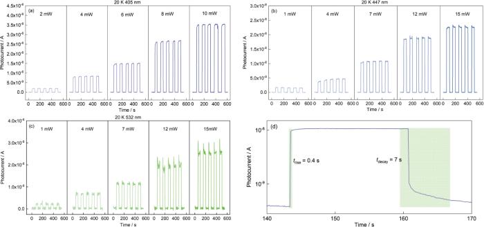
图4
器件在20 K的光电开关特性
Fig.4
Photoresponse switching characteristics of the device,the switching behavior under various laser illuminations are illustrated with (a) 405 nm, (b) 447 nm, and (c) 532 nm at a forward bias voltage of 4 V, (d) response time
3 结论
这种WSe2/BFO/Q2DEG混合异质结具有铁电调控下的CPC效应,在低温下具有可充电光电导和光电响应。温度低于60 K时,光生载流子的电荷存储量随着温度的降低呈指数级增长,失效温度为60 K。CPC效应具有宽光谱响应(405~808 nm),其响应强度与光子能量相关。短波长高能量的光子高效激发WSe2与BFO界面处的载流子,峰值电流可达250 μA。CPC效应存在于405~532 nm波长范围内,波长为808 nm时消失,响应阈值与WSe2带隙相匹配。施加0到-4 T的垂直磁场I-V回线完全重叠,表明载流子的存储和释放不受Zeeman效应或自旋极化的影响,适于强磁环境中的光电存储。
参考文献
Controlling many-body states by the electric-field effect in a two-dimensional material
[J].
Tuning Ising superconductivity with layer and spin-orbit coupling in two-dimensional transition-metal dichalcogenides
[J].
Systems simultaneously exhibiting superconductivity and spin-orbit coupling are predicted to provide a route toward topological superconductivity and unconventional electron pairing, driving significant contemporary interest in these materials. Monolayer transition-metal dichalcogenide (TMD) superconductors in particular lack inversion symmetry, yielding an antisymmetric form of spin-orbit coupling that admits both spin-singlet and spin-triplet components of the superconducting wavefunction. Here, we present an experimental and theoretical study of two intrinsic TMD superconductors with large spin-orbit coupling in the atomic layer limit, metallic 2H-TaS2 and 2H-NbSe2. We investigate the superconducting properties as the material is reduced to monolayer thickness and show that high-field measurements point to the largest upper critical field thus reported for an intrinsic TMD superconductor. In few-layer samples, we find the enhancement of the upper critical field is sustained by the dominance of spin-orbit coupling over weak interlayer coupling, providing additional candidate systems for supporting unconventional superconducting states in two dimensions.
Impact of moire superlattice on atomic stress and thermal transport in van der Waals heterostructures
[J].
Enhanced bulk photovoltaic effect in two-dimensional ferroelectric CuInP2S6
[J].
P-type electrical contacts for 2D transition-metal dichalcogenides
[J].
Shift current photovoltaic effect in a ferroelectric charge-transfer complex
[J].Shift current is a steady-state photocurrent generated in non-centrosymmetric single crystals and has been considered to be one of the major origins of the bulk photovoltaic effect. The mechanism of this effect is the transfer of photogenerated charges by the shift of the wave functions, and its amplitude is closely related to the polarization of the electronic origin. Here, we report the photovoltaic effect in an organic molecular crystal tetrathiafulvalene-p-chloranil with a large ferroelectric polarization mostly induced by the intermolecular charge transfer. We observe a fairly large zero-bias photocurrent with visible-light irradiation and switching of the current direction by the reversal of the polarization. Furthermore, we reveal that the travel distance of photocarriers exceeds 200 mu m. These results unveil distinct features of the shift current and the potential application of ferroelectric organic molecular compounds for novel optoelectric devices.
Small-voltage multiferroic control of two-dimensional magnetic insulators
[J].
Magnetoelectric coupling in multiferroic bilayer VS2
[J].
Recent advances in carbazole-based self-assembled monolayer for solution-processed optoelectronic devices
[J].
Hole mobility enhancement and p-doping in monolayer WSe2 by gold decoration
[J].
Vertically stacked multi-heterostructures of layered materials for logic transistors and complementary inverters
[J].Graphene has attracted considerable interest for future electronics, but the absence of a bandgap limits its direct applicability in transistors and logic devices. Recently, other layered materials such as molybdenum disulphide (MoS(2)) have been investigated to address this challenge. Here, we report the vertical integration of multi-heterostructures of layered materials for the fabrication of a new generation of vertical field-effect transistors (VFETs) with a room temperature on-off ratio > 10(3) and a high current density of up to 5,000 A cm(-2). An n-channel VFET is created by sandwiching few-layer MoS(2) as the semiconducting channel between a monolayer graphene sheet and a metal thin film. This approach offers a general strategy for the vertical integration of p- and n-channel transistors for high-performance logic applications. As an example, we demonstrate a complementary inverter with a larger-than-unity voltage gain by vertically stacking graphene, Bi(2)Sr(2)Co(2)O(8) (p-channel), graphene, MoS(2) (n-channel) and a metal thin film in sequence. The ability to simultaneously achieve a high on-off ratio, a high current density and a logic function in such vertically stacked multi-heterostructures can open up possibilities for three-dimensional integration in future electronics.
Mapping twist-tuned multiband topology in bilayer WSe2
[J].Semiconductor moiré superlattices have been shown to host a wide array of interaction-driven ground states. However, twisted homobilayers have been difficult to study in the limit of large moiré wavelengths, where interactions are most dominant. In this study, we conducted local electronic compressibility measurements of twisted bilayer WSe (tWSe) at small twist angles. We demonstrated multiple topological bands that host a series of Chern insulators at zero magnetic field near a "magic angle" around 1.23°. Using a locally applied electric field, we induced a topological quantum-phase transition at one hole per moiré unit cell. Our work establishes the topological phase diagram of a generalized Kane-Mele-Hubbard model in tWSe, demonstrating a tunable platform for strongly correlated topological phases.
Recent progress in strain engineering on van der Waals 2D materials: tunable electrical, electrochemical, magnetic, and optical properties
[J].
Material and device design of flexible perovskite solar cells for next-generation power supplies
[J].
Emergent multi-field interaction in a magnetic quasi-two-dimensional WSe2/SrCoO2.5/2DEG heterojunction
[J].
Chargeable photoconductivity in van der Waals heterojunctions of black phosphorus and quasi-two-dimensional electron gas
[J].Nowadays, there is a surge of research reports on photovoltaic cells and photodetectors based on van der Waals (vdW) heterojunction. However, there are very few reports on the simultaneous realization of photoelectric conversion and storage in a single device. Herein, a simple method was utilized to successfully prepare a van der Waals heterojunction with a chargeable photoconductivity (CPC) effect between black phosphorus and quasi-two-dimensional electron gas. After a single optical illumination, the device generated photocarriers and stored them for up to 5 days, followed by a bias voltage applied in the dark to release a large photocurrent of 1.0 mA and a current ratio of up to 10 before and after full optical charging. Firstly, experiments showed that the CPC effect critical temperature was approximately 100 K, which is 20 K higher than the highest temperature reported in the literature. Secondly, the CPC effect spectral range of the device increases from 405 nm-808 nm to 405 nm-1064 nm, including even general daylight, indicating that the device's responsivity and photon collection ability are more prominent. This discovery provides a new direction, to the best of our knowledge, for storage photoconductors and high-efficiency photoelectric storage devices.
BiFeO3 nanoparticles: the "Holy-Grail" of piezo-photocatalysts?
[J].
Switching the spin cycloid in BiFeO3 with an electric field
[J].Bismuth ferrite (BiFeO) is a multiferroic material that exhibits both ferroelectricity and canted antiferromagnetism at room temperature, making it a unique candidate in the development of electric-field controllable magnetic devices. The magnetic moments in BiFeO are arranged into a spin cycloid, resulting in unique magnetic properties which are tied to the ferroelectric order. Previous understanding of this coupling has relied on average, mesoscale measurements. Using nitrogen vacancy-based diamond magnetometry, we observe the magnetic spin cycloid structure of BiFeO in real space. This structure is magnetoelectrically coupled through symmetry to the ferroelectric polarization and this relationship is maintained through electric field switching. Through a combination of in-plane and out-of-plane electrical switching, coupled with ab initio studies, we have discovered that the epitaxy from the substrate imposes a magnetoelastic anisotropy on the spin cycloid, which establishes preferred cycloid propagation directions. The energy landscape of the cycloid is shaped by both the ferroelectric degree of freedom and strain-induced anisotropy, restricting the spin spiral propagation vector to changes to specific switching events.© 2024. The Author(s).
Dipolar wavevector interference induces a polar skyrmion lattice in strained BiFeO3 films
[J].Skyrmions can form regular arrangements, so-called skyrmion crystals (SkXs). A mode with multiple wavevectors q then describes the arrangement. While magnetic SkXs, which can emerge in the presence of Dzyaloshinskii-Moriya interaction, are well established, polar skyrmion lattices are still elusive. Here we report the observation of polar SkXs with a well-defined double-q state in ultrathin BiFeO films on LaAlO. The compressive strain induced by the LaAlO substrate yields a dipolar topological texture with a periodic arrangement of skyrmions. The square-like superstructure with a lattice constant of 2.68 nm features a periodic modulation of polarization fields and topological charge density. The film furthermore exhibits an enhanced electromechanical response with an increased converse piezoelectric coefficient (d) compared with SkX-free films. Transmission electron microscopy experiments in combination with phase-field simulations indicate that the dipole skyrmion texture results from the interference of two orthogonal single-q dipole patterns. We anticipate that the interference of multiple wavevectors may lead to a diversity of topological crystals with a variety of symmetries and lattice constants.© 2025. The Author(s), under exclusive licence to Springer Nature Limited.
Enhanced visible light photocatalytic activity of Gd-doped BiFeO3 nanoparticles and mechanism insight
[J].
The preparation and characterization of 1D multiferroic BFO/P(VDF-TrFE) composite nanofibers using electrospinning
[J].
Room temperature intrinsic ferromagnetism in epitaxial manganese selenide films in the monolayer limit
[J].Monolayer van der Waals (vdW) magnets provide an exciting opportunity for exploring two-dimensional (2D) magnetism for scientific and technological advances, but the intrinsic ferromagnetism has only been observed at low temperatures. Here, we report the observation of room temperature ferromagnetism in manganese selenide (MnSe ) films grown by molecular beam epitaxy (MBE). Magnetic and structural characterization provides strong evidence that, in the monolayer limit, the ferromagnetism originates from a vdW manganese diselenide (MnSe) monolayer, while for thicker films it could originate from a combination of vdW MnSe and/or interfacial magnetism of α-MnSe(111). Magnetization measurements of monolayer MnSe films on GaSe and SnSe epilayers show ferromagnetic ordering with a large saturation magnetization of ∼4 Bohr magnetons per Mn, which is consistent with the density functional theory calculations predicting ferromagnetism in monolayer 1T-MnSe. Growing MnSe films on GaSe up to a high thickness (∼40 nm) produces α-MnSe(111) and an enhanced magnetic moment (∼2×) compared to the monolayer MnSe samples. Detailed structural characterization by scanning transmission electron microscopy (STEM), scanning tunneling microscopy (STM), and reflection high energy electron diffraction (RHEED) reveals an abrupt and clean interface between GaSe(0001) and α-MnSe(111). In particular, the structure measured by STEM is consistent with the presence of a MnSe monolayer at the interface. These results hold promise for potential applications in energy efficient information storage and processing.
Two-dimensional itinerant ferromagnetism in atomically thin Fe3GeTe2
[J].
Proximity-induced ferromagnetism in graphene revealed by the anomalous hall effect
[J].
Impact of carrier recombination on fill factor for large area heterojunction crystalline silicon solar cell with 25.1% efficiency
[J].We have achieved a certified 25.1% conversion efficiency in a large area (151.9 cm2) heterojunction (HJ) crystalline Si (c-Si) solar cell with amorphous Si (a-Si) passivation layer. This efficiency is a world record in a both-side-contacted c-Si solar cell. Our high efficiency HJ c-Si solar cells are investigated from the standpoint of the effective minority carrier lifetime (τe), and the impact of τe on fill factor (FF) is discussed. The τe measurements of our high efficiency HJ c-Si solar cells reveal that τe at an injection level corresponding to an operation point of maximum power is dominated by the carrier recombination at the a-Si/c-Si interface. By optimization of the process conditions, the carrier recombination at the a-Si/c-Si interface is reduced, which leads to an improvement of the FF by an absolute value of 2.7%, and a conversion efficiency of 25.1% has been achieved. These results indicate that the reduction of carrier recombination centers at the a-Si/c-Si interface should be one of the most crucial issues for further improvement of FF even in the HJ c-Si solar cells with efficiency over 25%.
Design rules for high-efficiency both-sides-contacted silicon solar cells with balanced charge carrier transport and recombination losses
[J].
Scalable integration of hybrid high-κ dielectric materials on two-dimensional semiconductors
[J].
A mass transfer technology for high-density two-dimensional device integration
[J].
General low-temperature growth of two-dimensional nanosheets from layered and nonlayered materials
[J].Most of the current methods for the synthesis of two-dimensional materials (2DMs) require temperatures not compatible with traditional back-end-of-line (BEOL) processes in semiconductor industry (450 °C). Here, we report a general BiOCl-assisted chemical vapor deposition (CVD) approach for the low-temperature synthesis of 27 ultrathin 2DMs. In particular, by mixing BiOCl with selected metal powders to produce volatile intermediates, we show that ultrathin 2DMs can be produced at 280-500 °C, which are ~200-300 °C lower than the temperatures required for salt-assisted CVD processes. In-depth characterizations and theoretical calculations reveal the low-temperature processes promoting 2D growth and the oxygen-inhibited synthetic mechanism ensuring the formation of ultrathin nonlayered 2DMs. We demonstrate that the resulting 2DMs exhibit electrical, magnetic and optoelectronic properties comparable to those of 2DMs grown at much higher temperatures. The general low-temperature preparation of ultrathin 2DMs defines a rich material platform for exploring exotic physics and facile BEOL integration in semiconductor industry.© 2023. The Author(s).


