


OLED是一种在电场作用下将电能转化为光能的发光器件[1,2],具有轻薄、功耗低、对比度高、响应快速和柔性等优点[3~5],是新一代柔性显示和照明技术的首要候选者。OLED由透明阳极、空穴注入层、空穴传输层(HTL)、发光层、电子传输层、电子注入层和阴极构成[6]。优化设计OLED各功能层的厚度使发光层中的空穴与电子高效复合,可显著提高器件的性能。器件中的HTL将阳极产生的空穴传输到发光层中。2007年Khan等[7]发现,调控HTL的厚度可实现OLED器件中电荷的注入平衡,从而提高器件的效率。2009年Gan等[8]发现,增大HTL的厚度可将激子复合区向阴极方向移动、使光谱偏移。因此,调控HTL的厚度可提高OLED器件的性能。
具有较高空穴迁移率(10-2 cm2·V -1·s-1)的TAPC是一种典型的HTL材料[9~14],可使器件中的空穴载流子高效运输。同时,其良好的疏水性能阻止水分子和氧气渗入,提高器件的稳定性[15]。Wang等[16]使用40 nm厚的TAPC作为HTL,以铟锡氧化物(ITO)为透明电极,制备出QE为10.6%的绿光OLED器件。Hajime等[17]用35 nm厚的TAPC作为HTL,以ITO为透明电极,制备出EQE为15.8%的绿光OLED器件。Xu等[18]使用55 nm厚的TAPC作为HTL,制备出EQE为17.97%的绿光OLED器件。研究结果表明,TAPC HTL的厚度对刚性ITO基OLED器件的性能有显著的影响[17,19~23]。
透明电极材料的选择显著影响柔性OLED器件的性能。现有的多种电极材料,如银纳米线[24,25]、聚(3,4-乙烯二氧噻吩):聚苯乙烯磺酸盐(PEDOT:PSS)[26]和超薄金属[27]等具有优异的性能,在柔性OLED器件中都得到了应用[28~33]。石墨烯具有优异的光电性能,也可用作透明电极材料。厚度仅为0.34 nm的石墨烯,具有极高的本征载流子迁移率(2,000,000 cm2·V -1·s-1)[34]和高达97.7%的光透过率[35]。独特的结构和优异的光电性能使石墨烯可替代ITO透明电极成为制备柔性OLED器件的首选材料[32,36~40]。Zhang等[41]以石墨烯为阳极、以60 nm厚的TAPC为HTL,制备出首个发光面积为56 cm2的柔性绿光OLED器件。但是,石墨烯的光电性质、表面形貌和厚度等与ITO电极有较大的不同。为了实现TAPC在柔性石墨烯基OLED器件中的应用,还要系统研究TAPC厚度对器件性能的影响。鉴于此,本文以石墨烯为透明阳极、TAPC为空穴传输材料,用蒸镀法制备柔性绿光石墨烯基OLED(G-OLED)器件,研究蒸镀速率对TAPC薄膜表面形貌和TAPC厚度对器件发光性能的影响。
1 实验方法
1.1 三层石墨烯薄膜电极的制备
先用化学气相沉积(CVD)法在铜箔上生长石墨烯薄膜,使用甲烷作为碳源、氢气作为载气,生长温度为1000℃;将沉积了墨烯薄膜的铜箔(Cu/G)裁剪成截面为3 cm × 3 cm的小片,将一片Cu/G薄膜固定在旋涂台上,将聚甲基丙烯酸甲酯(PMMA)的乳酸乙酯溶液(质量分数为4%)旋涂在Cu/G薄膜片的表面,转速为2000 r/min,旋涂时间为60 s;在120℃下将PMMA膜固化15 min后冷却至室温;将旋涂PMMA的Cu/G放置在铜刻蚀液中刻蚀,得到PMMA/石墨烯;用聚对苯二甲酸乙二醇酯(PET)将PMMA/石墨烯转移至去离子水中清洗;然后将第二片Cu/G薄膜用胶带固定在PET上,用其捞取去离子水中的PMMA/石墨烯,烘干厚得到PMMA/石墨烯/石墨烯/Cu(PMMA/2L-G/Cu);将PMMA/2L-G/Cu转移至铜刻蚀剂中刻蚀后得到PMMA/2L-G,然后用去离子水清洗;重复上述Cu/G薄膜转移和刻蚀步骤,用丙酮清洗后得到PET/石墨烯/石墨烯/石墨烯(PET/3L-G)。
1.2 OLED器件的制备
制备OLED器件用的有机材料为TAPC、乙酰丙酮酸二(2-苯基吡啶)铱(Ir(ppy)2acac)、二(2-羟基苯基吡啶)合铍(Bepp2)、红菲咯啉(BPhen),其分子结构如图1所示。用真空蒸镀法制备结构如图2a所示的绿光G-OLED器件。先用PL-00-20W光线激光直写刻蚀机(沈阳赛普贝斯科技有限公司)将PET/3L-G图形化。将截面为3 cm × 3 cm的PET/3L-G样品刻蚀成具有“上下”与“左右”对称的“L型”作为透明电极。然后在PET/3L-G表面蒸镀10 nm MoO3作为空穴注入层、以不同厚度的TAPC作为HTL,用Ir(ppy)2(acac)和Bepp2进行双源共蒸出10 nm的Bepp2:Ir(ppy)2(acac)作为发光层,其中Bepp2与Ir(ppy)2(acac)的蒸镀速率比为10∶1。最后,依次蒸镀10 nm Bepp2作为空穴阻挡层、60 nm BPhen作为电子传输层、1 nm LiF作为电子注入层、100 nm Al作为阴极材料。如图2b所示,该器件的能级结构能促进空穴与电子的传输和复合,提高器件的性能。用主客掺杂方式制备发光层,主体材料Bepp2的LUMO能级比Ir(ppy)2(acac)大0.1 eV,有利于在主体材料Bepp2中形成的三线态激子通过德克斯特(Dexter)能量转移[42]转移到客体材料Ir(ppy)2(acac)中,实现载流子高效复合、辐射发光,以防止三线态-三线态能量湮灭。
图1
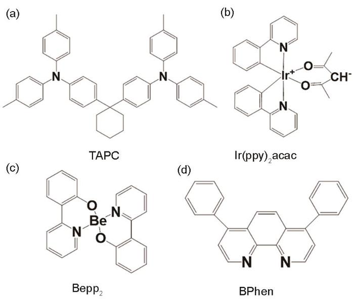
图1
OLED器件制备使用的有机材料
Fig.1
Organic materials used in OLED devices (a) Molecular structure of TAPC, (b) Ir(ppy)2acac, (c) Bepp2 and (d) BPhen
图2
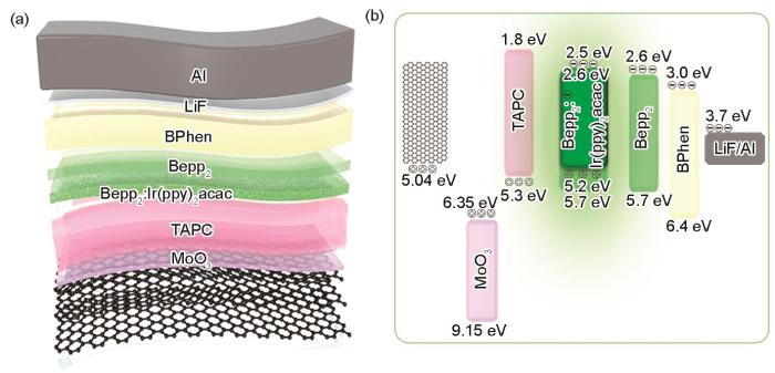
图2
G-OLED器件的结构和能级图
Fig.2
Device structure (a) and Energy level diagram (b) of the G-OLED
1.3 材料性能的表征
用MultiMode 8型高分辨扫描探针显微镜表征蒸镀前后PET/3L-G/MoO3/TAPC薄膜的表面形貌;使用RTS-9四探针测试仪测量弯曲过程中石墨烯电阻的变化;用Keithley 2450数字源表和PR-788光谱仪所组成的测试系统测量有不同厚度TAPC HTL的石墨烯基OLED器件的工作电压、电流、亮度、色坐标、电流密度、外量子效率(External quantum efficiency,EQE)、电流效率(Current efficiency,CE)、功率效率(Power efficiency,PE)等电学与光学性能。G-OLED器件的有效发光面积为2 mm ×2 mm。
在氮气环境手套箱中测试石墨烯电极和TAPC层厚度为70 nm的石墨烯基OLED器件在弯曲半径为R = 1 cm的弯折过程中其电阻和发光亮度的变化,以避免空气中水氧的侵入。
2 结果和讨论
2.1 TAPC蒸镀速率对TAPC层表面形貌的影响
TAPC的厚度为60 nm,分别以0.05 nm·s-1、0.1 nm·s-1和0.15 nm·s-1的速率在PET/3L-G/MoO3上蒸镀TAPC,制备出的PET/3L-G/MoO3/TAPC结构如图3所示。可以看出,未蒸镀TAPC层时PET/3L-G/MoO3结构的表面粗糙度为Ra = 3.45 nm,蒸镀速率为0.05 nm·s-1的TAPC层其表面粗糙度最低,为Ra = 2.52 nm。随着蒸镀速率提高到0.15 nm·s-1时,薄膜的粗糙度也随之增大到Ra = 2.58 nm。其原因是,蒸镀速率较低时TAPC镀料蒸发出的颗粒较小,能很好地填充石墨烯凹凸不平的表面,从而使其表面粗糙度降低。蒸镀速率较高时,镀料的气体分子剧烈地运动和碰撞,产生的高能粒子扰动薄膜表面而使表面粗糙度提高;但是,蒸镀速率的提高也使镀料的束流分散程度提高,使薄膜在待镀物表面的分布不均匀,因此沉积成膜后表面粗糙度较大。较大的粗糙度影响TAPC与相邻功能层的界面质量,进而使器件的漏电流增大。鉴于此,本文实验以0.05 nm·s-1的蒸镀速率制备TAPC层。
图3
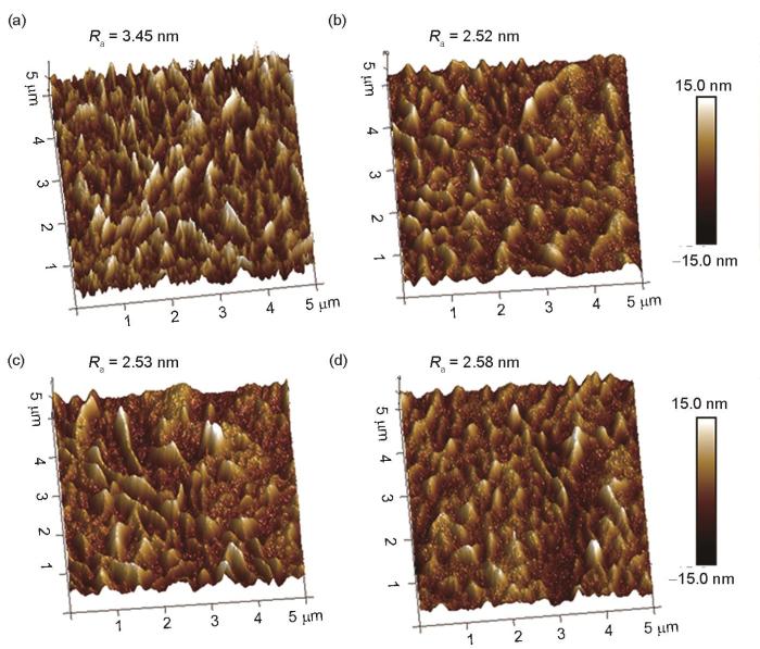
图3
不同蒸镀速率制备的60 nm厚TAPC层的表面形貌
Fig.3
Morphologies of PET/3L-G/MoO3 (a) and TAPC layer on PET/3L-G/MoO3 fabricated at evaporation rate of 0.05 nm·s-1(b), 0.1 nm·s-1 (c) and 0.15 nm·s-1 (d)
2.2 TAPC厚度对器件性能的影响
以0.05 nm·s-1的蒸镀速率在PET/3L-G/MoO3上制备不同厚度的TAPC层进而制备出G-OLED器件。图4a给出了TAPC层厚度不同的G-OLED器件的电流密度-电压(J-V)特性曲线。其中A、B、C和D分别为TAPC厚度为50、60、70和80 nm的G-OLED器件。可以看出,TAPC空穴传输层的厚度对器件的J-V特性有显著的影响。所有器件的电流密度随着器件电压的增大而增大,V = 9 V时器件A、B、C、D的电流密度分别为17.57、29.92、59.98和37.21 mA·cm-2。在电压相同的条件下器件的电流密度先随着厚度的增大而提高,当厚度达到80 nm时器件的电流密度下降。
图4
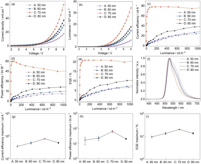
图4
OLED器件的J-V曲线、L-V曲线、CE-L曲线、PE-L曲线、EQE-L性能、电致发光的光谱图、CE最大值、PE最大值和EQE最大值
Fig.4
Device performance of OLED with different thickness of TAPC layers (a) current density-voltage (J-V) curve; (b) luminance-voltage (L-V) curve; (c) current efficiency-luminance (CE-L) curve; (d) power efficiency-luminance (PE-L) curve; (e) external quantum efficiency-luminance (EQE-L) curve; (f) electroluminescence spectra; (g) current effici-ency maximum; (h) power efficiency maximum; (i) external quantum efficiency maximum
图4b给出了不同TAPC厚度G-OLED器件的亮度-电压(L-V)特性曲线。结合表1中的相关性能参数可知,外加电压小于5 V时所有器件的亮度变化都不明显;当外加电压大于5 V时亮度快速提高。在电压相同的条件下,TAPC HTL厚度为70 nm的器件其亮度最大。V = 9 V时器件A、B、C、D的最大亮度分别达到5901、14260、34350、17650 cd·m-2。其主要原因是,随着TAPC层增厚由阳极和阴极注入并传输到发光层的空穴载流子与电子载流子逐步达到平衡,使电子与空穴充分结合形成激子而辐射发光,因此器件的亮度逐渐提高。但TAPC层过厚时部分空穴载流子在传输过程中湮灭,从而使器件的亮度降低。
表1 G-OLED器件的性能
Table 1
| Performance | A | B | C | D |
|---|---|---|---|---|
| Lmax / cd·m-2 | 5901 | 14260 | 34350 | 17650 |
| CDmax / mA·cm-2 | 17.57 | 29.92 | 59.98 | 37.22 |
| CEmax / cd·A-1 | 33.58 | 48.19 | 78.10 | 50.56 |
| PEmax / lm·W-1 | 12.43 | 18.80 | 60.04 | 21.93 |
| EQEmax / % | 9.27 | 12.91 | 21.02 | 13.67 |
| λ / nm | 530 | 528 | 525 | 528 |
| CIE (x, y) | 0.3802, | 0.3486, | 0.3140, | 0.3611, |
| 0.5900 | 0.6169 | 0.6386 | 0.6074 |
和
其中L为亮度,J为电流密度,V是器件工作电压。可以看出,器件的CE决定于其亮度和电流密度。因此,亮度越大和电流密度越高,则器件的电流效率越高。器件A、B、C、D的亮度在1000 cd·m-2以内,其最大电流效率CEmax分别为23.98、26.7、78.1和50.5 cd·A-1。在2 V~9 V的测试电压范围内,器件A、B、C、D的CEmax分别为33.58、48.19、78.10和50.56 cd·A-1;而器件的常用工作电压为5 V~6 V,由图4b可知,在此条件下各器件在相同的电压下其电流密度较为接近,因此亮度较大的器件其CE也比较大。由此可见,器件A的最大电流其效率最小,而器件C的最大电流其效率最大。由
图4f给出了不同TAPC HTL厚度G-OLED器件的发光光谱。结合表1可见,所有器件都具有相似的光谱曲线。器件C在λ = 525 nm处显示出Ir(ppy)2(acac)材料激发波长的电致发光峰,而器件A、B、D在λ = 529 nm附近显示出电致发光,因为电荷注入不平衡使峰位偏移。需要指出的是,器件A、B、D位于λ = 560 nm附近出现了较为明显的肩峰。根据文献[43],TAPC的三线态能级
如图4g~i所示,TAPC厚度为50 nm、60 nm、70 nm与80 nm的OLED器件,其最大电流效率、功率效率与外量子效率的变化趋势基本相同,其性能随着TAPC层厚度的增大而提高;但是,当厚度继续增加到80 nm时器件的性能开始降低。如图5a~d所示,器件的表面粗糙度均方根呈现出与性能相似的变化趋势,但是其最大峰高则随TAPC厚度的增加而逐渐减小,达到70 nm后表面最大起伏基本不变,有利于缓解电荷注入与电荷传输效率的降低。低粗糙度的TAPC层改善了OLED器件的界面接触,提供了更多的空穴传输通道,从而使空穴在HTL层中的传输效率提高。此外,随着TAPC厚度的增大器件的串联电阻随之增大;只有TAPC的厚度适当,器件的电流密度才能达到最大(图4a)。为了进一步验证TAPC的厚度对器件的影响,在相同条件下制备了单空穴器件(图5e)。如图5f所示,器件的TAPC层厚度达到70 nm时,单空穴器件的电流密度达到最大。这表明,此时器件中的空穴载流子最多,空穴更容易传输。但是,当TAPC层的厚度增加至80 nm时器件的空穴载流子反而减少。其原因是,空穴载流子迁移距离过大,使部分空穴载流子在传输过程中湮灭。以上结果表明,TAPC厚度为70 nm的OLED器件其性能更优异。
图5
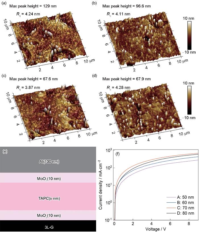
图5
不同TAPC厚度的OLED器件的形貌
Fig.5
Morphology of OLED devices with different thickness of TAPC (a) 50 nm; (b) 60 nm; (c) 70 nm; (d) 80 nm. (e) the structure of hole-only device; (f) current density-voltage characteristics of hole-only devices
2.3 优化条件下柔性绿光OLED器件的性能
图6a给出了以70 nm厚的TAPC为HTL制备的G-OLED器件C的CIE色谱图及其与器件A、B、D的对比。可以看出,器件C的发光颜色位于(0.3140,0.6386),为典型的绿光;而器件A,B,D的TAPC层厚度不匹配,使部分激子在Bepp2层复合,受激发后辐射出黄光。因此,这些器件的发光颜色都位于(0.3488,0.6163)附近,颜色略微偏黄。
图6
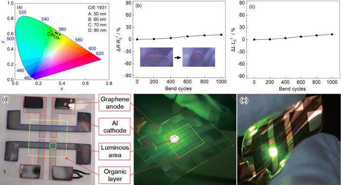
图6
柔性绿光G-OLED器件的性能
Fig.6
Performance of flexible green G-OLED devices (a) CIE chromatogram of OLED device; (b) surface resistance change of graphene film after a thousand bending; (c) brightness change of OLED device after a thousand bending; (d) photograph and emission performance of flexible green OLED devices fabricated by using 70 nm-thick TAPC as HTL, lighting area of 2 mm × 2 mm; (e) photograph of lighting OLED device under bending
综上所述,器件C的性能最佳,其发光亮度、电流效率、功率效率和外量子效率都最高。但是,OLED器件工作时受到波导、全反射和表面等离子基元效应的影响,约有82%的光困在器件内[45]。本文调控空穴传输层TAPC的厚度,制备出EQE高达21.02%的G-OLED器件。
3 结论
以石墨烯为透明阳极、以TAPC为HTL可制备柔性绿光G-OLED器件。蒸镀速率为0.05 nm·s-1时制备的TAPC薄膜其表面粗糙度较低,有利于提高器件界面的质量。在保持其他各功能层厚度不变的条件下,TAPC厚度为70 nm的G-OLED器件性能最佳:外量子效率达到21.02%、电流效率达到78.10 cd·A-1、功率效率达到60.04 lm·W-1、最大亮度达到34350 cd·m-2。这种器件具有优异的柔韧性,将其反复弯折后器件仍能稳定工作,即使在弯折过程中仍能均匀发光。
参考文献
Recent advances in oled optical design
[J].
Efficient bipolar blue aiegens for high-performance nondoped blue oleds and hybrid white oleds
[J].
Transflective device with a transparent organic light-emitting diode and a reflective liquid-crystal device
[J].
— A high‐transmittance transflective device based on a hybrid structure consisting of a transparent organic light‐emitting diode (OLED) stacked on top of a reflective liquid‐crystal device (RLCD) was conceptually demonstrated. By placing the transparent OLED on top of a vertically aligned LCD operated under normally black mode, a transmittance as high as 75.7% was obtained due to the asymmetric emission characteristics of a transparent OLED. To further improve the performance in the transmissive mode, a polarizer‐free LCD was used, which yielded an ultra‐high transmittance (82.2% overall).
Quantitative analysis of the efficiency of oleds
[J].
High-contrast tandem organic light-emitting devices employing semitransparent intermediate layers of lif/al/c60
[J].
Long-lived flexible displays employing efficient and stable inverted organic light-emitting diodes
[J].
Highly efficient organic electroluminescent diodes realized by efficient charge balance with optimized electron and hole transport layers
[J].
Electroluminescence characteristics of organic thin film pumped by photoluminescence
[J].
Highly efficient phosphorescent organic light-emitting diodes using a homoleptic iridium(iii) complex as a sky-blue dopant
[J].
Efficient red organic electroluminescent devices by doping platinum(ii) schiff base emitter into two host materials with stepwise energy levels
[J].In this work, organic electroluminescent (EL) devices with double light-emitting layers (EMLs) having stepwise energy levels were designed to improve the EL performance of a red-light-emitting platinum(II) Schiff base complex. A series of devices with single or double EML(s) were fabricated and characterized. Compared with single-EML devices, double-EML devices showed improved EL efficiency and brightness, attributed to better balance in carriers. In addition, the stepwise distribution in energy levels of host materials is instrumental in broadening the recombination zone, thus delaying the roll-off of EL efficiency. The highest EL current efficiency and power efficiency of 17.36 cd/A and 14.73 lm/W, respectively, were achieved with the optimized double-EML devices. At high brightness of 1000 cd/m², EL efficiency as high as 8.89 cd/A was retained.
High-efficiency phosphorescent white organic light-emitting diodes with stable emission spectrum based on rgb separately monochromatic emission layers
[J].
High performance top-emitting and transparent white organic light-emitting diodes based on al/cu/tcta transparent electrodes for active matrix displays and lighting applications
[J].
Color stable and low driving voltage white organic light-emitting diodes with low efficiency roll-off achieved by selective hole transport buffer layers
[J].
Low-driving-voltage blue phosphorescent organic light-emitting devices with external quantum efficiency of 30%
[J].
Conjugated small molecule for efficient hole transport in high-performance p-i-n type perovskite solar cells
[J].
Combining intrinsic (blue) and exciplex (green and orange-red) emissions of the same material (oct) in white organic light-emitting diodes to realize high color quality with a cri of 97
[J].By simultaneously combining blue intrinsic emission and green, orange-red exciplex emissions of the same material (OCT), three color white OLEDs were demonstrated with the maximum color rendering index reaching 97.
High-efficiency organic light-emitting diodes with fluorescent emitters
[J].Fluorescence-based organic light-emitting diodes have continued to attract interest because of their long operational lifetimes, high colour purity of electroluminescence and potential to be manufactured at low cost in next-generation full-colour display and lighting applications. In fluorescent molecules, however, the exciton production efficiency is limited to 25% due to the deactivation of triplet excitons. Here we report fluorescence-based organic light-emitting diodes that realize external quantum efficiencies as high as 13.4-18% for blue, green, yellow and red emission, indicating that the exciton production efficiency reached nearly 100%. The high performance is enabled by utilization of thermally activated delayed fluorescence molecules as assistant dopants that permit efficient transfer of all electrically generated singlet and triplet excitons from the assistant dopants to the fluorescent emitters. Organic light-emitting diodes employing this exciton harvesting process provide freedom for the selection of emitters from a wide variety of conventional fluorescent molecules.
Highly simplified tandem organic light-emitting devices incorporating a green phosphorescence ultrathin emitter within a novel interface exciplex for high efficiency
[J].
Dependence of light-emitting characteristics of blue phosphorescent organic light-emitting diodes on electron injection and transport materials
[J].
Luminous efficiency enhancement in blue phosphorescent organic light-emitting diodes with an electron confinement layers
[J].
Multilayered graphene anode for blue phosphorescent organic light emitting diodes
[J].In this work, we report on blue organic light emitting devices (OLEDs), which have multilayered graphene as its anode. Our graphene films have been grown catalytically and transferred to the support. The fabricated blue OLEDs with graphene anode showed outstanding external quantum efficiency of 15.6% and power efficiency of 24.1 lm/W at 1000 cd/m2. Weak oxygen plasma treatments on graphene film surfaces improved the injection property between the anode and hole injection layer.
Bipolar host materials for high efficiency phosphorescent organic light emitting diodes: Tuning the homo/lumo levels without reducing the triplet energy in a linear system
[J].
Efficient red, green, blue and white organic light-emitting diodes with same exciplex host
[J].
A solution processed flexible nanocomposite substrate with efficient light extraction via periodic wrinkles for white organic light-emitting diodes
[J].
Junction-free electrospun ag fiber electrodes for flexible organic light-emitting diodes
[J].
Enhanced light extraction from oleds fabricated on patterned plastic substrates
[J].
Silver/germanium/silver: An effective transparent electrode for flexible organic light-emitting devices
[J].
Unlocking the full potential of organic light-emitting diodes on flexible plastic
[J].
Extremely efficient flexible organic light-emitting diodes with modified graphene anode
[J].
Approaching ultimate flexible organic light-emitting diodes using a graphene anode
[J].
High-performance organic light-emitting diode with substitutionally boron-doped graphene anode
[J].
Ultra-smooth and robust graphene-based hybrid anode for high-performance flexible organic light-emitting diodes
[J].
Efficient deep-blue electroluminescent devices based on a novel β-diketone zinc complex
[J].
Wafer-scale synthesis of graphene on sapphire: Toward fab-compatible graphene
[J].
Fine structure constant defines visual transparency of graphene
[J].There are few phenomena in condensed matter physics that are defined only by the fundamental constants and do not depend on material parameters. Examples are the resistivity quantum, h/e2 (h is Planck's constant and e the electron charge), that appears in a variety of transport experiments and the magnetic flux quantum, h/e, playing an important role in the physics of superconductivity. By and large, sophisticated facilities and special measurement conditions are required to observe any of these phenomena. We show that the opacity of suspended graphene is defined solely by the fine structure constant, a = e2/hc feminine 1/137 (where c is the speed of light), the parameter that describes coupling between light and relativistic electrons and that is traditionally associated with quantum electrodynamics rather than materials science. Despite being only one atom thick, graphene is found to absorb a significant (pa = 2.3%) fraction of incident white light, a consequence of graphene's unique electronic structure.
A transparent, flexible, low-temperature, and solution-processible graphene composite electrode
[J].
Emerging transparent electrodes based on thin films of carbon nanotubes, graphene, and metallic nanostructures
[J].
Graphene oxide/graphene vertical heterostructure electrodes for highly efficient and flexible organic light emitting diodes
[J].The relatively high sheet resistance, low work function and poor compatibility with hole injection layers (HILs) seriously limit the applications of graphene as transparent conductive electrodes (TCEs) for organic light emitting diodes (OLEDs). Here, a graphene oxide/graphene (GO/G) vertical heterostructure is developed as TCEs for high-performance OLEDs, by directly oxidizing the top layer of three-layer graphene films with ozone treatment. Such GO/G heterostructure electrodes show greatly improved optical transmittance, a large work function, high stability, and good compatibility with HIL materials (MoO3 in this work). Moreover, the conductivity of the heterostructure is not sacrificed compared to the pristine three-layer graphene electrodes, but is significantly higher than that of pristine two-layer graphene films. In addition to high flexibility, OLEDs with different emission colors based on the GO/G heterostructure TCEs show much better performance than those based on indium tin oxide (ITO) anodes. Green OLEDs with GO/G heterostructure electrodes have the maximum current efficiency and power efficiency, as high as 82.0 cd A(-1) and 98.2 lm W(-1), respectively, which are 36.7% (14.8%) and 59.2% (15.0%) higher than those with pristine graphene (ITO) anodes. These findings open up the possibility of using graphene for next generation high-performance flexible and wearable optoelectronics with high stability.
Wafer‐scale graphene anodes replace indium tin oxide in organic light‐emitting diodes
[J].
Rational molecular design enables efficient blue tadf-oleds with flexible graphene substrate
[J].
Rosin-enabled ultraclean and damage-free transfer of graphene for large-area flexible organic light-emitting diodes
[J].The large polymer particle residue generated during the transfer process of graphene grown by chemical vapour deposition is a critical issue that limits its use in large-area thin-film devices such as organic light-emitting diodes. The available lighting areas of the graphene-based organic light-emitting diodes reported so far are usually <1 cm(2). Here we report a transfer method using rosin as a support layer, whose weak interaction with graphene, good solubility and sufficient strength enable ultraclean and damage-free transfer. The transferred graphene has a low surface roughness with an occasional maximum residue height of about 15nm and a uniform sheet resistance of 560 Omega per square with about 1% deviation over a large area. Such clean, damage-free graphene has produced the four-inch monolithic flexible graphene-based organic light-emitting diode with a high brightness of about 10,000 cd m(-2) that can already satisfy the requirements for lighting sources and displays.
Energy transfer catalysis mediated by visible light: Principles, applications, directions
[J].Harnessing visible light to access excited (triplet) states of organic compounds can enable impressive reactivity modes. This tutorial review covers the photophysical fundamentals and most significant advances in the field of visible-light-mediated energy transfer catalysis within the last decade. Methods to determine excited triplet state energies and to characterize the underlying Dexter energy transfer are discussed. Synthetic applications of this field, divided into four main categories (cyclization reactions, double bond isomerizations, bond dissociations and sensitization of metal complexes), are also examined.
Ultra-simple hybrid white organic light-emitting diodes with high efficiency and cri trade-off: Fabrication and emission-mechanism analysis
[J].
High efficiency yellow fluorescent organic light emitting diodes based on m-mtdata/bphen exciplex
[J].
