


石墨烯的性能优异,在电子器件、导热材料和复合材料等领域有潜在的应用价值[1~6]。因此,近年来关于石墨烯材料的研究受到了高度重视。但是,石墨烯是零带隙半导体[6~8],没有发光特性。氧化石墨烯(Graphite oxide,GO)是石墨烯重要的衍生物之一,是规模化生产石墨烯的原料。GO和石墨烯的结构差异很大,GO内部有羟基、羧基和环氧基等大量氧化官能团。氧化官能团破坏了石墨烯片层的 π 共轭体系,使其电学性质和光学性质发生了巨大变化,由导电(石墨烯)变为绝缘(GO)[9~12]并具有光催化活性[13~15]。特别是sp2C/sp3C的交替分布打开了石墨烯的带隙,使其具有发光性能。GO发光分布在可见光和近红外波段,可用于生物检测[16,17]和荧光标记[18]。目前对氧化石墨烯光学性质的研究刚刚展开,对其能带结构的认识和发光机理的理解还很不深入。本文根据光致发光光谱、变温发光光谱和吸收光谱,研究GO的发光机制和不同激发波长与变温条件下的发光光谱,以揭示不同局域态的发光行为。
1 实验方法
1.1 实验用材料和仪器
天然鳞片石墨(325目);微孔滤膜(醋酸纤维酯,直径50 mm,孔径0.22 μm)。
inVia型发光光谱仪(PL);Lambda900型紫外-可见吸收光谱仪(UV-Vis)。
1.2 氧化石墨烯的制备
用改进的Hummers法[19],将天然鳞片石墨通过超声辅助液相氧化法制备氧化石墨烯(GO)。用真空抽滤法制备GO薄膜,改变过滤GO溶液的量或浓度,调节薄膜的厚度。分别在488 nm、514 nm和830 nm激发条件下测试GO薄膜的荧光光谱。在514 nm和830 nm激发条件下研究GO薄膜的原位变温发光。
2 结果和讨论
2.1 氧化石墨的吸收特性
其中E0为urbach能,表征带尾态的宽度,与材料的无序程度相关。根据
图1

图1
GO的紫外-可见吸收光谱和GO吸收光谱的Tauc拟合图
Fig.1
UV-Vis absorption spectra of GO (a) and corresponding Tauc plot (b)
2.2 常温条件下GO的发光特性
图2给出了GO分别在Eex =488 nm(2.53 eV>Eopt),Eex=514 nm(2.41 eV>Eopt)和Eex =830 nm(1.49 eV<Eopt)激发条件下的光致发光光谱(PL)。GO的PL发射峰都具有非常宽的谱带;随着激发光能量的降低发射峰中心波长逐渐红移,半峰宽(FWHM)变窄。
图2

图2
GO在488 nm,514 nm和830 nm激发波长下的发光光谱和GO 发射峰的中心波长(左)和半峰宽(右)与激发光波长的关
Fig.2
PL spectra of GO for excitation at Eex =488 nm, Eex =514 nm and Eex =830 nm (a) and the dependences as the function of excitation wavelengths: (left) peak wavelength and (right) FWHM of PL spectra (b)
图3

用多量子阱的能带结构可解释GO的发光特征。sp2C团簇π-π*间的带隙与尺寸相关,碳团簇的尺寸越小带隙越宽。GO的片层结构中存在不同尺寸的sp2C区域,因此分布着非常多的局域状态,可由吸收光谱中较大的urbach能证明。由于共振吸收效应,激发光能量与发光中心带隙能量相同时吸收最强。在不同激发条件下,因共振吸收效应参与的发光中心不同,因此随着激发能量降低发光的主峰位置红移。同时,随着激发能量的降低可被激发的发光中心减少,使发光峰的半峰宽变窄。
2.3 GO的变温发光性质
图4给出了GO发光强度与温度的关系。在514.5 nm和830 nm激发条件下和80 K~300 K范围内,GO的发光强度降低一个数量级,强度变化的转折点分别出现在220 K(Eex =514.5 nm)和160 K(Eex =830 nm)。GO的发光强度随温度的变化在一个数量级内,与非晶碳发光随温度的变化关系相似[23,30,31]。以往的研究表明,在非晶碳材料体系中,即使具有较高的缺陷密度(发光猝灭中心密度大),温度对发光强度的影响仍然较小[31]。其原因是,电子-空穴对被sp3C区域的高势垒限制在局域的碳团簇中,使电子-空穴的波函数交叠变大,大大提高了发生辐射跃迁的几率[30,32]。相反,sp3C势垒层被破坏后,由于体系缺陷的密度较高,在声子辅助下电子快速转移缺陷处复合,在室温下很难观察到发光现象,如a-Si1-x Cx:H(x<0.09)[32]。制备过程中的强氧化作用,使GO中存在大量缺陷态(如碳空位)。但是,高势垒sp3C区域对sp2C团簇的限域效应,限制了电子到缺陷态的复合,使辐射跃迁几率提高,在室温下即可观察到发光现象。氧化官能团(高势垒区)被破坏后,如氧化石墨烯被还原,虽然GO内仍然存在小尺寸的sp2C团簇(发光中心)仍然能观察到发光现象[33]。
图4

图4
两种不同激发条件下GO相对发光强度的温度依赖性:(a) Eex =514 nm; (b) Eex =830 nm
Fig.4
Temperature dependence of the relative PL intensity of GO at two different exciting conditions: (a) Eex =514 nm; (b) Eex =830 nm
在不同激发波长条件下,变温发光随着温度的变化呈现不同的变化趋势。在514 nm激发下在80~220 K,GO的发光强度受温度的影响较小,温度≥220 K时发光强度明显降低;在830 nm激发下在80~300 K,GO的发光强度随着温度的降低而降低,温度≥160 K时发光强度降低的速率变大。利用Arrhenius方程[34],可拟合得到发光猝灭的热激活能
其中T为温度,kB为波尔兹曼常数,I0为0 K附近的PL谱积分强度,A为常数,Ea 为热激活能。拟合结果为:Eex =514 nm,热激活能Ea =119 MeV(图5a);Eex =830 nm,热激活能Ea =63 MeV(图5b)。这表明,与Eex =830 nm相比,在Eex =514 nm激发下参与发光的sp2C团簇的热稳定性更高,发生温度猝灭所需的热激活能高达56 MeV。根据GO的多量子阱结构,可解释不同激发波长下的变温发光。由于共振效应,不同能量的光激发不同尺寸的局域态(sp2C团簇)。与Eex =830 nm相比,Eex =514 nm激发的sp2C团簇尺寸较小。在多量子阱结构中,由于量子尺寸效应,sp2C团簇尺寸越小能级间隔越大,热猝灭需要的参与的声子数目增加,因此尺寸越小发光强度受温度的影响越小。
图5
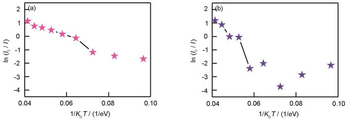
图5
光致发光强度与1/KBT之间的关系
Fig.5
Relationship between relative PL intensity and 1/KBT, exciting at Eex =514 nm (a) and Eex =830 nm (b)
3 结论
用多量子阱结构能解释GO的发光特性。GO的发光来自于片层内的sp2C团簇。sp2C团簇被高势垒的氧化官能团(sp3C)包围,形成了多量子阱结构。GO内有不同尺寸的sp2C团簇,由于量子尺寸效应sp2C团簇的带隙与尺寸相关。因此GO的发光呈现出对激发波长的依赖,尺寸越小带隙越宽,温度对发光强度的影响越小。
参考文献
Graphene-based ultracapacitors
[J].
The surface area of a single graphene sheet is 2630 m(2)/g, substantially higher than values derived from BET surface area measurements of activated carbons used in current electrochemical double layer capacitors. Our group has pioneered a new carbon material that we call chemically modified graphene (CMG). CMG materials are made from 1-atom thick sheets of carbon, functionalized as needed, and here we demonstrate in an ultracapacitor cell their performance. Specific capacitances of 135 and 99 F/g in aqueous and organic electrolytes, respectively, have been measured. In addition, high electrical conductivity gives these materials consistently good performance over a wide range of voltage scan rates. These encouraging results illustrate the exciting potential for high performance, electrical energy storage devices based on this new class of carbon material.
Graphene-based electrochemical supercapacitors
[J].
Chaotic dirac billiard in graphene quantum dots
[J].The exceptional electronic properties of graphene, with its charge carriers mimicking relativistic quantum particles and its formidable potential in various applications, have ensured a rapid growth of interest in this new material. We report on electron transport in quantum dot devices carved entirely from graphene. At large sizes (>100 nanometers), they behave as conventional single-electron transistors, exhibiting periodic Coulomb blockade peaks. For quantum dots smaller than 100 nanometers, the peaks become strongly nonperiodic, indicating a major contribution of quantum confinement. Random peak spacing and its statistics are well described by the theory of chaotic neutrino billiards. Short constrictions of only a few nanometers in width remain conductive and reveal a confinement gap of up to 0.5 electron volt, demonstrating the possibility of molecular-scale electronics based on graphene.
Design, fabrication, and characterization of Hg2+ sensorbased on graphite oxide and metallic nanoclusters
[J].
Photocatalytic activities of heterostructured TiO2-graphene porous microspheres prepared by ultrasonic spray pyrolysis
[J].
Photo-assisted preparation and patterning of large-area reduced graphene oxide-TiO2 conductive thin film
[J].
First-principle study of energy band structure of armchair graphene nanoribbons
[J].
Nanometer scale spectral imaging of quantum emitters in nanowires and its correlation to their atomically resolved structure
[J].
Experimental observation of the quantum Hall effect and Berry's phase in graphene
[J].
Photoluminescence and band gap modulation in graphene oxide
[J].
Blue photoluminescence from chemically derived graphene oxide
[J].
Hydrothermal route for cutting graphene sheets into blue-luminescent graphene quantum dots
[J].
Synthesis and characterization of graphene film via photo-chemical reduction of graphene oxide
[J].
Waveband-dependent photochemical processing of graphene oxide in fabricating reduced graphene oxide film and graphene oxide-Ag nanoparticles film
[J].
Photodegradation of antibiotic in environmental water by graphene oxide modulation bismuth molybdate under visible light irradiation
[J].
Biosensors based on graphene oxide and its biomedical application
[J].
Logic and reversible dual DNA detection based on the assembly of graphene oxide and DNA-templated quantum dots
[J].
Nano-graphene oxide for cellular imaging and drug delivery
[J].
Preparation of graphitic oxide
[J].
Processable aqueous dispersions of graphene nanosheets
[J].
Highly conducting graphene sheets and Langmuir-Blodgett films
[J].
The long-wavelength edge of photographic sensitivity and of the electronic absorption of solids
[J].
The effects of nitrogen partial pressure on the microstructure of amorphous carbon nitride films
[J].
Spatio-temporal analysis of the electric field-induced solid-state reduction dynamics of graphene oxide thin films for controlled band-gap modulation
[J].
Bonding defects and optical band gaps of DLC films deposited by microwave surface-wave plasma CVD
[J].
Phonon-Assisted Electroluminescence from Metallic Carbon Nanotubes and Graphene
[J].We report on light emission from biased metallic single-wall carbon nanotube (SWNT), multiwall carbon nanotube (MWNT) and few-layer graphene (FLG) devices. SWNT devices were assembled from tubes with different diameters in the range 0.7-1.5 nm. They emit light in the visible spectrum with peaks at 1.4 and 1.8 eV. Similar peaks are observed for MWNT and FLG devices. We propose that this light emission is due to phonon-assisted radiative decay from populated pi* band states at the M point to the Fermi level at the K point. Since for most carbon nanotubes as well as for graphene the energy of unoccupied states at the M point is close to 1.6 eV, the observation of two emission peaks at approximately 1.6 +/- approximately 0.2 eV could indicate radiative decay under emission or absorption of optical phonons, respectively.
Urbach tail and gap states in hydrogenated a-SiC and a-SiGe alloys
[J].
Making Graphene Luminescent by Oxygen Plasma Treatment
[J].We show that strong photoluminescence (PL) can be induced in single-layer graphene using an oxygen plasma treatment. The PL is spatially uniform across the flakes and connected to elastic scattering spectra distinctly different from those of gapless pristine graphene. Oxygen plasma can be used to selectively convert the topmost layer when multilayer samples are treated.
A Green Approach to the Synthesis of Graphene Nanosheets
[J].
π-bonded clusters in amorphous carbon materials
[J].
Diamond-like amorphous carbon
[J].
Photoluminescence of amorphous hydrogenated silicon-carbon (a-SiC:H) films
[J].
Water-triggered luminescent "nano-bombs" based on supra-(carbon nanodots)
[J].
