


与其它贵金属(Au、Pt、Pd)相比,Ag具备无毒且价格较低、易制备、化学性质稳定等优点[16,17]。同时,光沉积法成本较低和工艺简单,通过调整沉积时间、光强和前驱体溶液配比即可在室温下实现Ag纳米粒子的可控制备[18~20]。目前,关于用金属Ag修饰半导体以加快电子-空穴对分离已有大量的研究工作。Liu等[21]通过将化学气相沉积与热蒸发相结合制备了Ag修饰ZnO阵列,能有效分离电子-空穴对。且与未修饰ZnO相比,其紫外探测性能显著提高。Devi等[22]合成了一种Ag修饰CeO2纳米棒光电探测器,Ag纳米粒子修饰能显著抑制CeO2纳米棒电子-空穴对的复合并提升其捕获电子的能力。Joshna等[23]制备的Ag修饰TiO2纳米管(TiO2 NTs),金属Ag显著减少了电子-空穴对的复合,Ag纳米粒子修饰的TiO2 NTs的光电流是纯TiO2 NTs的120倍。同时,在各种SnSe纳米结构材料中一维SnSe纳米管具有高电子传输效率、几何异向性和量子限域效应,更有利于提高红外探测性能[24~26]。因此,使用Ag修饰的SnSe纳米管有望制备出高性能红外探测器。本文用光沉积法在SnSe纳米管表面修饰金属Ag纳米粒子,在室温下合成Ag修饰SnSe(Ag/SnSe)纳米管并以Pt为对电极组装红外探测器,研究其在模拟红外光(830 nm)照射下的红外探测性能、光响应速度和循环稳定性,并讨论其机理。
1 实验方法
1.1 Ag/SnSe纳米管的制备
以Se纳米线为模板,用溶液法制备SnSe纳米管[26],然后将0.02 g的SnSe纳米管加到30 mL的0.05 mol/L 硝酸银溶液中并磁力搅拌使其分散均匀;用波长为365 nm的紫外光照射溶液,光沉积15 min后自然沉降5 min。然后将得到的样品用去离子水清洗并离心分离出Ag/SnSe纳米管,重复2次后将其在烘箱中低温干燥。
1.2 Ag/SnSe纳米管红外探测器的制备
将制备出的Ag/SnSe纳米管分散在无水乙醇中,然后旋涂到FTO导电面后烘干,将这一过程重复三次,获得Ag/SnSe纳米管薄膜。以负载在FTO表面的Ag/SnSe纳米管薄膜为工作电极,以镀Pt的FTO为对电极,通过热封膜将工作电极和对电极相连接,中间注入聚硫电解质溶液后密封。
1.3 性能表征
使用扫描电子显微镜(SEM,Hitachi SU-70)及附带的X射线能谱仪(EDS)表征样品形貌和化学成分。用透射电子显微镜(TEM,FEI,Tecnai G2 F20)和高分辨透射电子显微镜(HRTEM)观测样品的形貌。用X射线衍射仪(XRD,Bruker D8 Advance)表征样品的晶体结构。将组装好的Ag/SnSe纳米管探测器与Keithley 2400数字源表连接,使用830 nm的光作为模拟红外光源,测试其红外探测性能。
2 结果与讨论
图1
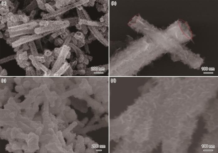
图1
SnSe纳米管和Ag/SnSe纳米管的SEM照片
Fig.1
SEM images of SnSe nanotubes (a, b) and Ag/SnSe nanotubes (c, d)
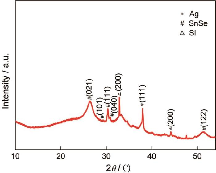
用EDS分析Ag/SnSe纳米管的元素组成,结果如图2所示。图中有源于SnSe纳米管的Se和Sn元素的特征峰,最强峰来自测试支撑Si衬底(用于样品形貌观察)。在2.99 keV处出现了Ag元素的特征峰,表明在SnSe纳米管表面沉积了Ag纳米粒子。
图2

图3
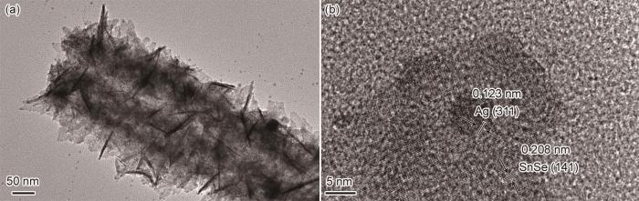
图3
Ag/SnSe纳米管的TEM和高分辨TEM照片
Fig.3
TEM (a) and high resolution TEM (b) images of Ag/SnSe nanotube
图4
在无外加偏压条件下用830 nm的光作为红外光模拟光源,开启红外光照射10 s后关闭红外光10 s作为一个测试周期,研究了Ag/SnSe纳米管探测器对红外光的探测性能,其结果如图5所示。在无红外光照射时Ag/SnSe纳米管红外探测器为静默状态,光电流密度几乎为零;开启红外光后器件瞬间产生光电流并快速攀升至最大值120 nA/cm2,然后逐渐稳定。关闭红外光后,光电流迅速衰减并恢复到初始状态。经过6次开关循环,电流密度曲线没有明显的变化,这表明,所组装的探测器具备高电流密度和较好的耐用性。同时,器件能在无偏压条件下稳定工作,表明其具有自供能特性。在相同的实验条件下测试了SnSe纳米管红外探测器的性能,其光电流密度只有46 nA/cm2,比Ag/SnSe纳米管红外探测器的光电流密度降低了61%。这表明,Ag纳米粒子修饰明显提高了SnSe纳米管探测器对红外光的探测性能。
图5

图5
SnSe纳米管和Ag/SnSe纳米管红外探测器在开/关红外光照射下的电流密度曲线
Fig.5
Time dependent current response of the SnSe and Ag/SnSe nanotubes infrared photodetector (IRPD) measured under on/off of IR light illumination
图6
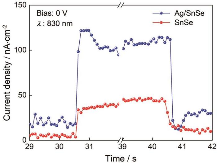
图6
SnSe纳米管和Ag/SnSe纳米管红外探测器单个周期的光电响应特征曲线
Fig.6
Single-cycle photocurrent response of the IRPD based on SnSe and Ag/SnSe nanotubes
Ag/SnSe纳米管红外探测器的机理如图7所示。Ag/SnSe纳米管独特的鱼鳞状中空结构和大比表面积,显著提高了对红外光的吸收能力,进而提高了对红外光的利用效率。用红外光照射时SnSe纳米管吸收的光子能量高于其带隙,因此光生电子激发后从价带跃迁至导带并在价带留下空穴。电子-空穴对的快速复合严重影响了SnSe纳米管探测器的效率。而在SnSe表面负载Ag纳米粒子后,金属Ag与SnSe纳米管表面发生肖特基接触产生肖特基势垒,进而出现内建电场。在光生电子从SnSe表面迁至单质Ag的过程中促进载流子的分离,抑制了光生电子-空穴对的复合。同时,随着SnSe纳米管和电解液间电子-空穴对的分离[30],电子通过外部电路迁移至Pt电极并与电解液中的S x2-反应生成S2-和S x-12-。生成的S2-在电解液中扩散至SnSe纳米管与其表面的空穴反应生成S单质,S与S x-12-进一步反应生成S x2-[31]。S x2-和S2-没有被消耗而持续循环,使光生电子通过外电路产生电流。因此,Ag/SnSe纳米管红外探测器能实现对红外光的自供能探测。关闭红外光后没有光生电子产生,Ag/SnSe纳米管红外探测器迅速恢复到初始状态。
图7
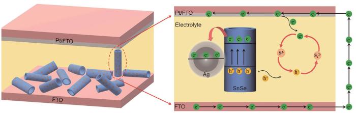
图7
Ag/SnSe纳米管红外探测器的原理
Fig.7
Schematic illustration of the possible IR detection mechanism of the Ag/SnSe nanotubes IRPD
3 结论
用光沉积法将Ag纳米颗粒沉积在鱼鳞状中空SnSe纳米管表面,在室温下制备Ag/SnSe纳米管。Ag/SnSe纳米管表面粗糙致密,在表面能观察到微小的Ag纳米粒子。与SnSe纳米管探测器相比,用Ag修饰的SnSe纳米管红外探测器的光电流密度提高了约160%(达到120 nA/cm2)、光响应速度也明显改善、上升时间缩短至0.109 s、下降时间缩短至0.086 s,且具有较高的循环稳定性。
参考文献
Infrared detector array with PLZT thick films on silicon-based microstructure tunnels
[J].
Si基微绝热结构PLZT厚膜红外探测器阵列
[J].
MBE grown antimonide mid-infrared lasers and photodetectors
[J].
用分子束外延制备红外锑化物激光器和探测器材料
[J].

用固态源分子束外延方法, 在GaSb衬底上成功地生长出四元系III-V族锑化物单层、多量子阱和激光器、探测器结构材料, 并用这些材料制备了2μm波段室温准连续脊波导AlGaAsSb/InGaAsSb多量子阱.
Electromagnetic absorber converting radiation for multifunction
[J].
High performance visible-near-infrared PbS-quantum-dots/indium Schottky diodes for photodetectors
[J].
A surface state-controlled, high-performance, self-powered photovoltaic detector based on an individual SnS nanorod with a symmetrical electrode structure
[J].
Flexible SnSe photodetectors with ultrabroad spectral response up to 10.6 μm enabled by photobolometric effect
[J].
All‐layered 2D optoelectronics: a high-performance UV-vis-NIR broadband SnSe photodetector with Bi2Te3 topological insulator electrodes
[J].
Self-powered, highly sensitive, high-speed photodetection using ITO/WSe2/SnSe2 vertical heterojunction
[J].
Photoresponse improvement in liquid-exfoliated SnSe nanosheets by reduced graphene oxide hybridization
[J].
High photoresponsivity and broadband photodetection with a band-engineered WSe2/SnSe2 heterostructure
[J].
An electrochemical strategy to incorporate nitrogen in nanostructured TiO2 thin films: modification of bandgap and photoelectrochemical properties
[J].
Preparation of Zn-doped TiO2 nanotubes electrode and its application in pentachlorophenol photoelectrocatalytic degradation
[J].
2D SnSe/Si heterojunction for self-driven broadband photodetectors
[J].
Fabrication and catalytic properties of Co-Ag-Pt nanoparticle-decorated titania nanotube arrays
[J].
A highly efficient Ag-ZnO photocatalyst: synthesis, properties, and mechanism
[J].
Fabrication of flexible self-powered UV detectors based on ZnO nanowires and the enhancement by the decoration of Ag nanoparticles
[J].
Preparation of highly uniform Ag/TiO2 and Au/TiO2 supported nanoparticle catalysts by photodeposition
[J].Photodeposition of Ag nanoparticles on commercial TiO2 particles and nanoparticles was performed in order to provide direct visualization of the spatial distribution of photoactive sites on sub-micrometer-scale and nanoscale TiO2 particle surfaces and to create materials for potential catalytic applications. HRTEM (high-resolution transmission electron microscopy) and HAADF-STEM (high-angle annular dark-field scanning transmission electron microscopy) were used to characterize these materials. The size and spatial distributions of the Ag nanoparticles on the commercial TiO2 were not uniform; the concentration of Ag was higher on grain boundaries and at the edges of these submicrometer particles. In the case of TiO2 nanoparticles, the size distribution of the Ag nanoparticles deposited was relatively uniform and independent of irradiation time and photon energy. The amount of Ag deposited on TiO2 nanoparticles was at least 6 times higher than that on the commercial samples for comparable irradiation conditions. Compared to the case of Ag photodeposition, the difference in the amount of Au photodeposited on TiO2 particles and nanoparticles was even greater, especially at low precursor concentrations. Photodeposition on TiO2 nanoparticles is suggested as a potential method for the preparation of Au/TiO2 catalysts, as loadings in excess of 10 wt % of uniform 1 nm metal particles were achieved in this work.
Photodeposition of Ag or Pt onto TiO2 nanoparticles decorated on step edges of HOPG
[J].
Effects of Ag-photodeposition on photocurrent of an ITO electrode modified by a hybrid film of TiO2 nanosheets
[J].
Ag nanoparticles@ZnO nanowire composite arrays: an absorption enhanced UV photodetector
[J].
Plasmon-induced Ag decorated CeO2 nanorod array for photodetector application
[J].
Fast response of UV photodetector based on Ag nanoparticles embedded uniform TiO2 nanotubes array
[J].
Wafer-size growth of 2D layered SnSe films for UV-Visible-NIR photodetector arrays with high responsitivity
[J].
High performance humidity sensor and photodetector based on SnSe nanorods
[J].
A facile solution synthesis of scaly-like hollow SnSe nanotubes for self-powered infrared sensor
[J].
Green synthesis of silver nanoparticles using Rhodobacter sphaeroides
[J].
Synthesis of silver microfibers with ultrahigh aspect ratio by galvanic replacement reaction
[J].
An overview on emerging photoelectrochemical self-powered ultraviolet photodetectors
[J].
High-performance self-powered UV photodetectors based on TiO2 nano-branched arrays
[J].
An integrated approach to realizing high-performance liquid-junction quantum dot sensitized solar cells
[J].Solution-processed semiconductor quantum dot solar cells offer a path towards both reduced fabrication cost and higher efficiency enabled by novel processes such as hot-electron extraction and carrier multiplication. Here we use a new class of low-cost, low-toxicity CuInSexS2-x quantum dots to demonstrate sensitized solar cells with certified efficiencies exceeding 5%. Among other material and device design improvements studied, use of a methanol-based polysulfide electrolyte results in a particularly dramatic enhancement in photocurrent and reduced series resistance. Despite the high vapour pressure of methanol, the solar cells are stable for months under ambient conditions, which is much longer than any previously reported quantum dot sensitized solar cell. This study demonstrates the large potential of CuInSexS2-x quantum dots as active materials for the realization of low-cost, robust and efficient photovoltaics as well as a platform for investigating various advanced concepts derived from the unique physics of the nanoscale size regime.
