


自2006年首次报道与聚变相关的He离子辐照下金属钨(W)表面生长W纳米丝结构以来[1],与W纳米丝相关的研究工作成为等离子体材料辐照损伤领域的研究热点[2,3]。W纳米丝,是在高温下将He离子注入到W中生成的纳米纤维状结构。W纳米丝相互交联,在聚变堆偏滤器靶板上形成多孔的微结构使偏滤器部件传热性能降低,同时影响在边界局域模(ELM)条件下诱导的温度分布[4]。因此,研究W纳米丝的形成机制及其在不同辐照参数下的稳定性对偏滤器部件的优化设计以及W基面向等离子体材料的发展有重要的意义。大量研究结果表明,在900~2000 K范围内大于30 eV的He离子能量才能在W表面产生W纳米丝结构层[5~7]。辐照参数的影响使W纳米丝直径的量级为几十至几百纳米,W纳米丝层的厚度为几十纳米至几微米[4]。W纳米丝的生长过程,与给定温度下He离子辐照剂量密切相关[8]。He泡驱动的W纳米丝生长机制,已被广泛接受[9~13]。注入的He原子在多晶W晶格间隙中扩散、聚集形成He团簇并在W表层产生He纳米气泡。He泡的长大挤压周围的W原子,产生间隙W原子并扩散,从而改变多晶W结构[9,10]。W体相中He泡的生长非常缓慢,但是不断增加的He泡内压使He泡向W表面扩散并在表面破裂。这种情况,使W表层的表面积增加并促进W纳米丝的生长。W纳米丝通过纤维尖端向外生长,W纳米丝层厚度的不断增大使He离子注入到W体相中的概率降低,从而影响了W纳米丝的生长速度[11~13]。本文研究W纳米纤维在He离子辐照过程中的不稳定性。
1 实验方法
辐照实验用多晶钨方片的尺寸为10 mm×10 mm×2 mm,纯度高于99.5%。辐照前对W片进行机械抛光,使其表面粗糙度小于0.1 μm。将抛光后的W片在1373 K真空(真空度为1.0×10⁻⁴ Pa)退火2 h。
在大功率材料辐照实验平台上用He离子辐照多晶W生成W纳米丝。实验时,将高纯He通入平台的真空腔室内,用频率为2 MHz的射频电源耦合在石英管内产生高密度的He等离子体[14]。在样品上施加-30 eV负偏压,以控制He离子能量为50 eV。放电功率为9.5 kW,离子流强为1.7×10²²/m2·s,辐照剂量为8.0×1025/m2,辐照温度为1500 K。在该条件下多晶W表面生成均匀的纳米丝层结构,其厚度为3.6 μm。
在低功率材料辐照实验平台上用He离子溅射W纳米丝[14],用能量为150 eV的He离子对已生长W纳米丝的样品进行间歇式辐照,放电功率为200 W,辐照温度为400 K,离子流强为2.0×10²⁰/m2·s,辐照剂量间隔为3.0×1023/m2,最大辐照剂量为1.0×1025/m2。
用扫描电子显微镜(S4800, HITACHI)分析样品的表面形貌变化。同时进行了平行实验,辐照剂量分别为1.2×1024/m2,2.4×1024 /m2,3.6×1024 /m2,5.5×1024 /m2和1.0×1025 /m2。用SEM分析平行实验中W纳米丝层厚度变化,用分析天平(XSE105DU,精度0.1 mg)测试平行实验中辐照前后W样品的质量损失,用透射电子显微镜(JEM-2100, JEOL)观察平行实验中W纳米丝的微观形貌和内部缺陷的分布。
2 结果和讨论
2.1 钨纳米丝的表面形貌
图1给出了辐照后W表面纳米丝的扫描电镜照片,He离子间歇式辐照温度为400 K,能量为150 eV。辐照前W丝的分布比较均匀,W表面单位面积内W丝密度较高,随着辐照剂量的增大,W丝的分布变得不均匀,单位面积内W丝的密度明显降低,W丝的直径显著增大。
图1
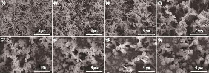
图1
间歇式He离子辐照后W纳米丝表面的SEM照片
Fig.1
SEM analysis of the surface morphology of W fuzz irradiated by intermittent He ion with different fluence, magnification is 40 K (a) 0/m2, (b) 3.0×10²³ /m2, (c) 1.2×1024 /m2, (d) 2.4×1024 /m2, (e) 3.6×1024 /m2, (f) 5.5×1024 /m2, (g) 7.5×1024 /m2, (h) 1.0×1025 /m2
为进一步分析W丝表面微结构演变,用高分辨SEM观察了W丝的形貌,如图2所示,SEM的放大倍数为150 K。辐照前W丝的平均直径约为20 nm,W丝的形态饱满,W丝与W丝之间互相交联成网状结构。辐照剂量为3.0×10²³ /m2时,W丝表面出现了尺寸为3~5 nm的细小孔洞。辐照剂量提高到1.2×1024 /m2时W丝表面的孔洞消失,W丝出现塌陷和合并,W丝边缘不再圆润而出现棱角。随着辐照剂量的继续提高W丝之间的交联程度降低,W丝继续合并堆叠、直径增大。辐照剂量提高到1.0×1025/m2时W丝与W丝之间不再交联,W丝变成顶部细、根部粗的结构,顶部W丝的直径约为30~40 nm,根部直径约为200~300 nm。
图2

图2
间歇式He离子辐照后W纳米丝表面的高分辨SEM照片
Fig.2
High resolution SEM analysis of the surface morphology of W fuzz irradiated by intermittent He ion with different fluence, magnification is 150 K (a) 0/m2, (b) 3.0×10²³ /m2, (c) 1.2×1024 /m2, (d) 2.4×1024 /m2, (e) 3.6×1024 /m2, (f) 5.5×1024 /m2, (g) 7.5×1024 /m2, (h) 1.0×1025 /m2
2.2 W纳米丝截面的形貌
图3a~d给出了平行实验中He离子辐照后W丝截面的SEM照片。原始样品的W丝层呈均匀网状分布,W丝与W丝之间相互交联,W丝顶部与根部直径相差不大。用辐照剂量为2.4×1024 /m2的He离子辐照后样品表层约1 μm深度范围内的W丝横向交联程度明显降低,W丝顶端成直立形貌。辐照剂量提高到5.5×1024 /m2,W丝的直立形貌从表层延伸到2 μm深度范围,表层W丝合并成簇状。随着辐照剂量提高到1.0×1025 /m2,W丝直立形貌从表层一直延伸到根部,W丝根部直径明显大于顶端直径,呈现锥型形貌。图3e给出了W丝层厚度随辐照剂量变化的统计曲线。原始W丝层厚度约3.6 μm,但是随着辐照剂量的提高W丝层的厚度急剧减小,辐照剂量为1.0×1025 /m2时W丝层厚度约为2.0 μm。这表明,能量为150 eV的He离子辐照对W丝层产生显著的溅射作用。在该条件下He离子辐照能量已远大于W原子的溅射阈值能(100~120 eV),高能He离子与W表面原子发生高频碰撞而使W表层原子发生溅射。随着He离子辐照剂量的增加溅射作用从表层向下逐渐延伸,而溅射出来的W原子沉积在临近的W丝外表面或W丝根部,使W丝合并生长并最终呈现锥型形貌。
图3

图3
间歇式He离子辐照后W纳米丝截面的SEM照片和W丝层的厚度随辐照剂量的变化
Fig.3
SEM analysis of the effect of intermittent He ion irradiation with different fluence on the cross-section morphology of W fuzz (a~d)and the curve of W fuzz layer thickness versus He+ fluence (e) (a) 0/m2, (b) 2.4×1024 /m2, (c) 5.5×1024 /m2, (d) 1.0×1025 /m2
2.3 He离子辐照对钨丝溅射率的影响
图4

图4
W丝样品的质量损失和溅射率与He离子辐照剂量的关系
Fig.4
Mass loss of W fuzz and sputtering yields of W sample as a function of H ion energy
当辐照离子剂量低于5.5×1024 /m2时溅射率几乎保持恒定,约为1.0×10-5 W/He+;辐照剂量提高到1.0×1025/m2样品的溅射率小幅度增加到1.7×10-5 W/He+。其原因是,随着辐照剂量的提高W纳米丝表面结构遭到刻蚀,但是内部的交联网状结构仍然存在。这种网状结构可避免高能He+继续侵蚀W的基底。当W丝变成锥形结构时W丝与W丝之间交联的网状结构几乎消失,对W基底的保护作用减弱,使样品的溅射率小幅度提高。但是He离子与W丝样品的作用过程非常复杂,既有溅射又有再沉积,溅射和再沉积相互竞争又相互制约,其结果是溅射率没有大幅度的改变。
2.4 He离子辐照后W丝的形貌
用TEM观察了不同剂量He离子辐照后W纳米丝的表面形貌及内部缺陷分布,结果在图5中给出。可以看出,原始W丝纤维边界圆润清晰,内部可见随机分布的He泡,其直径为5~30 nm。原始W丝经能量为150 eV、剂量为1.2×1024 /m2的He离子辐照后,在W丝边界附近出现浅色包层结构,包层与W丝外壁紧密结合在一起。这种包层结构,是W纳米丝被高能He离子溅射产生的W原子随机沉积在W纳米丝外壁产生的。继续提高He离子辐照剂量,则溅射出来的W原子继续沉积在W丝外壁上使外壁的包层结构变厚。同时,W纳米丝变细且内部的He泡密度降低。其原因是,高能He离子溅射使W丝的壁变薄直至内部He泡破裂,He原子从He泡中溢出使W丝塌陷。塌陷的W丝与周围的W丝合并生长,并与再沉积的W原子合并生长。溅射与再沉积的协同作用,使W丝最终演变成内部几乎为实心的锥形结构W丝。图5f左上角给出了对W丝外壁较薄位置进行的TEM电子衍射分析。结果表明,衍射图样为同心圆点阵结构。这进一步表明,再沉积生长的W结构为多晶W结构。
图5

图5
用不同剂量He离子辐照后W丝的透射电镜照片
Fig.5
TEM analysis the surface topography of W fuzz at different He ion fluence (a) 0/m2, (b) 1.2×1024 /m2, (c) 2.4×1024 /m2, (d) 3.6×1024 /m2, (e) 5.5×1024 /m2, (f) 1.0×1025 /m2
3 结论
用150 eV的He离子在400 K辐照W纳米丝,先在表层发生溅射,随着辐照剂量的增加溅射逐渐向W纳米丝根部延伸,溅射出来的W原子随机沉积在相邻的W纳米丝外壁或W纳米丝根部并伴随着W纳米丝内部He泡破裂,W丝合并生长。溅射与再沉积的协同作用使W纳米丝的网状交联结构消失,最终演变成顶部细根部粗的锥型结构。这些结果表明,He离子辐照使W纳米丝的结构极不稳定。
参考文献
Formation of nanostructured tungsten with arborescent shape due to helium plasma irradiation
[J].
He-ion induced surface morphology change and nanofuzz growth on hot tungsten surfaces
[J].
He Plasma Assisted Preparation of Nanostructure Tungsten Materials
[J].
Nanostructure tungsten materials were successfully prepared by He plasma assisted methods. The effects of ions fluences and discharge power on the surface morphology of tungsten were investigated. Scanning electron microscopy and tapping mode atomic force microscopy were used to characterize the sample topography and surface roughness under different discharge condition. At the discharge power of 6 kW and ion energy of 220 eV, it showed that the tungsten surface formed the nano pinhole structure and then the pore size gradually increased with increasing ion fluences. When the ion fluence increased to 1.0×1026 ionsm-2, the sample surface formed nano tungsten fuzz. The cross section analysis also showed that the nano structure layer thickness increases with the increase of irradiation ion flunece. High-resolution scanning electron microscope analysis found that there are a large number of nanoHe bubble at the interface of tungsten fuzz root and tungsten bulk, which gives the direct evidence that the tungsten fuzz forming is derived from He bubble. This work is of great significance for the further understanding the formation mechanism of nano tungsten fuzz.
He等离子体辅助的纳米钨结构材料的制备
[J].利用He等离子体辅助的方法制备了纳米钨结构材料,采用扫描电子显微镜、轻敲模式原子力显微镜对不同辐照离子剂量和功率变化条件下处理的样品形貌、表面粗糙度等特征进行了分析。结果表明, 在放电功率为6 kW, 离子能量为220 eV条件下, 钨表面先出现纳米孔结构, 随着离子辐照剂量的增加, 纳米孔径逐渐增加, 辐照剂量为1.0×10<sup>26</sup> ionsm<sup>-2</sup>时, 样品表面呈现密集的无序分布的纳米丝结构层,纳米结构层的厚度也随辐照剂量的增加而增加。高分辨扫描电子显微镜的测试结果表明纳米丝根部与钨基体界面处存在大量的纳米级He泡, 由此给出了纳米钨丝是由He泡演化而来的直接证据。
The challenges of plasma material interations in nuclear fusion Devices and potential solutions
[J].
Formation process of tungsten nanostructure by the exposure to helium plasma under fusion relevant plasma conditions
[J].
TEM observation of the growth process of helium nanobubbles on tungsten: nanostructure formation mechanism
[J].
Comparison of tungsten nano-tendrils grown in alcator c-mod and linear plasma devices
[J].
The effect of fusion-relevant He ion flux on the evolution of He nano-bubbles in W
[J].
The evolution of He nanobubbles in tungsten under fusion-relevant He ion irradition conditions
[J].
Competing kinetics and He bubble morphology in W
[J].
Model of fuzz formation on a tungsten surface
[J].
Material mixing during fuzz formation in W and Mo
[J],
Modeling W fuzz growth over polycrystalline W due to He ion irradiations at an elevated temperature
[J].
Nanostructured fuzz growth on tungsten under low-energy and high-flux He irradiation
[J].We report the formation of wave-like structures and nanostructured fuzzes in the polycrystalline tungsten (W) irradiated with high-flux and low-energy helium (He) ions. From conductive atomic force microscope measurements, we have simultaneously obtained the surface topography and current emission images of the irradiated W materials. Our measurements show that He-enriched and nanostructured strips are formed in W crystal grains when they are exposed to low-energy and high-flux He ions at a temperature of 1400 K. The experimental measurements are confirmed by theoretical calculations, where He atoms in W crystal grains are found to cluster in a close-packed arrangement between {101} planes and form He-enriched strips. The formations of wave-like structures and nanostructured fuzzes on the W surface can be attributed to the surface sputtering and swelling of He-enriched strips, respectively.
