


钛酸铅(PbTiO3, PTO)是典型的钙钛矿铁电氧化物,具有较强的极化强度、较低的介电常数和较高的居里温度[7],钛酸铅薄膜在存储和传感等领域有广阔的应用前景。高密度存储器件和高灵敏度传感器件要求薄膜具有优异的铁电压电性能,而性能的优化和提高需要调控薄膜的微结构(如取向和晶粒尺寸)。生长薄膜的衬底显著影响PTO薄膜的取向生长和织构[8~13],其机理主要是晶格失配产生的应力。添加中间层(种子层[14,15],缓冲层[16]或模板层[17])可诱导PTO薄膜的择优取向,这取决于中间层的取向[16]及其导致的形核能的变化[14]。Lu等[18]的实验结果表明,热处理温度影响PTO薄膜的晶粒尺寸,在700℃和620℃退火的PTO薄膜其平均晶粒尺寸分别为210 nm和130 nm。其中大晶粒(210 nm)薄膜中的几乎所有晶粒都包含90o畴,但是小晶粒(130 nm)薄膜中的大部分晶粒中没有90o畴。小晶粒薄膜具有更大的矫顽场和更小的介电常数[19],二者的相变温度分别为480℃和460℃[20]。大量工作研究了PTO薄膜的取向生长,但大都集中在取向对性能的影响,对薄膜生长机制的研究不够深入。同时,对PTO薄膜的晶粒尺寸调控研究也比较少,对晶粒形核和长大的过程仍不很清楚。因此,需要寻求一种简单有效的方法,同时实现取向和晶粒尺寸的调控,并构建PTO薄膜的生长机制和结构演化的关系。
1 实验方法
1.1 材料的制备
用水热法制备单晶和单畴的纳米片[23],用溶胶凝胶法制备PTO薄膜。分别以醋酸铅(Pb(CH3COO)2)和钛酸四正丁酯(Ti(C4H9O)4,TBOT)为铅源和钛源、以浓度为0.5 mol/L的乙二醇甲醚(HOCH2CH2OCH3)为溶剂以醋酸(CH3COOH, HAc)为催化剂、以甲酰胺(CHONH2)为表面活性剂、以乙酰丙酮(HAcAc)为螯合剂,调节Ti:Pb:HAc:HAcAc:CHONH2=1:1.1:10:1:0.2,其中Ti源的浓度为5 mmol。先将醋酸和甲酰胺溶于乙二醇甲醚并搅拌均匀,加入醋酸铅和纳米片(0.2%~8%,摩尔比)后在80℃加热搅拌均匀,得到Pb源溶液。将TBOT溶于乙酰丙酮后在80℃加热搅拌均匀后得到Ti源溶液,将其加入Pb源溶液中搅拌形成稳定溶胶。用旋涂法制膜:将溶液滴加在Si衬底上并使其以3000 r/min的转速旋转30 s,然后在室温下干燥20 min,接着在200℃热处理10 min后再在400℃热解30 min。重复甩膜直至热解6~12次达到所需薄膜厚度,最后在650℃退火1 h成膜。
1.2 材料的表征
使用X射线衍射仪(XRD,Rigaku D/max-RA)表征纳米片和PTO薄膜的物相,CuKα靶,入射波长λ=0.15406 nm。用扫描电子显微镜(SEM,Hitachi SU-70)表征纳米片和PTO薄膜的形貌和结构,最高加速电压为30 KV。用聚焦离子束(FIB)加工技术切割出包含Si衬底和PTO薄膜的截面样品,并用Ticnai G2 F20型透射电子显微镜(TEM)表征薄膜的断面微结构,最高加速电压为200 kV。用树脂包埋方式制备纳米片的切片,并用球差矫正透射电镜(FEI Titan G2 80-200 Chemi STEM)进行原子级的环形明场像(ABF-STEM)表征,以分析纳米片的极化方向并计算极化强度值。使用Nicolet 380型红外光谱仪(FTIR)测试红外光谱,使用DT Q600型热分析仪进行差热和热重分析。使用Empyrean 200895型原位X射线衍射仪(in-situ XRD)测得XRD谱,扫描步长为0.02o,扫描速度为4~15℃/min,测试温度范围为400~650℃,升温速率为2℃/min,达到指定温度后保温15 min以使温度稳定。
2 结果和讨论
2.1 PTO纳米片的表征
图1给出了PTO纳米片的微结构、相变温度和铁电极化表征。图1a给出了纳米片的SEM照片,可见纳米片有规则的矩形外貌,其横向尺寸为600~1100 nm,厚度约为150 nm。纳米片的差热和热重曲线,如图1b所示。位于486.97℃的吸热峰对应PTO纳米片的相变,即由铁电四方相转变为顺电立方相。这表明,纳米片的相变温度为486.97℃,与块体的相变温度即居里温度(490℃)接近。低于相变温度时,纳米片为四方铁电相。通过ABF-STEM观察到Pb、Ti和O的原子像,可见Ti和O原子相对于相邻四个Pb原子的中心有一定的位移(图1c)。根据二者的相对位移量(图1d)计算[24]出纳米片的极化强度约为67 μC/cm2,与块体的值接近[25]。
图1
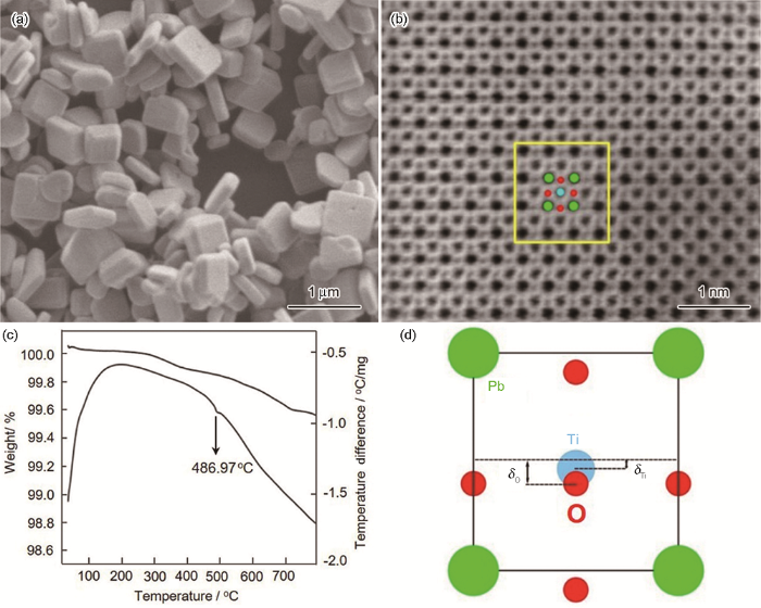
图1
纳米片的SEM照片、DTA和TGA曲线和横截面的ABF-STEM图
Fig.1
SEM image of PTO nanoplates(a),DTA/TGA curves of PTO nanoplates(b) and Cross-sectional ABF-STEM image of PTO nanoplates(c), where Pb (green), Ti (blue) and O (red) atoms have been marked and Unit-cell projection of tetragonal PTO along (010) direction(d), the displacement of Ti and O atoms with respect to the center of the Pb atoms along the c-axis are denoted as δTi and δO
2.2 PTO薄膜的结构
图2a给出了添加不同含量(0,0.2%,0.5%,0.8%,摩尔比)纳米片薄膜的XRD谱。可以看出,制备出的薄膜是钙钛矿结构的四方相PTO(JCPDS 70-0746),其中位于28.51o的峰是Si衬底的(111)衍射峰,没有杂质相。由图2b可见,随着纳米片含量的提高(100)峰相对于最强峰(101)的强度逐渐提高。定义(100)取向的比例α=I(100)/I(101),其中I(100)和I(101)分别为(100)和(101)峰的强度。α随着纳米片浓度的变化,如图2c所示。当纳米片含量由0提高到0.8%时α由78.3%增大到90.4%,说明纳米片的加入有利于PTO薄膜(100)取向生长。纳米片的XRD图谱中(100)峰强远低于(101)[23],说明纳米片含量的提高没有使PTO薄膜(100)取向的比例提高。
图2
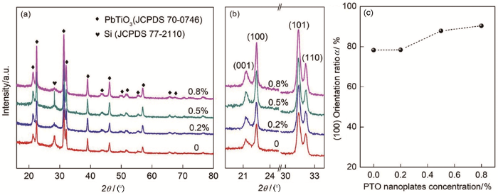
图2
添加不同含量纳米片制备的PTO薄膜的XRD图谱及其图中19-35o部分的放大图和(100)取向比例与纳米片含量的关系
Fig.2
XRD spectra of PTO film synthesized with adding different concentrations of nanoplates (a); Enlarged part of 19~35o in (a) (b) and (100) orientation ratio of PTO films as a function of nanoplates concentration (c)
添加不同含量(0,0.2%,0.5%,0.8%,摩尔比)纳米片的PTO薄膜的形貌,如图3所示。可以看出,添加纳米片使PTO薄膜中的晶粒尺寸发生了显著的变化。没有纳米片的薄膜表面由100~200 nm的晶粒组成,添加0.2%的纳米片后晶粒尺寸增大到~500 nm;纳米片含量提高到0.5%和0.8%,晶粒的平均尺寸达到1~2 μm。铁电薄膜的平均晶粒尺寸增大后具有更高的铁电畴迁移速率,使薄膜的介电常数进一步提高,矫顽场降低[26]。从图3b和c还可以看到,在单个晶粒中出现条状纹路(图3b和c中黑色虚线框和箭头所指),可能是小颗粒取向排列拼接聚合的痕迹,而在未添加纳米片的薄膜中没有观察到类似现象(图3a)。这表明,纳米片的加入使PTO薄膜的生长发生变化。
图3
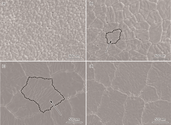
图3
添加不同含量纳米片的PTO薄膜的SEM照片
Fig.3
SEM images of PTO films synthesized by sol-gel method with adding different concentrations of nanoplates (a) 0; (b) 0.2%; (c) 0.5%; (d) 0.8%
XRD和SEM的结果表明,纳米片的加入显著改变了PTO薄膜的取向和晶粒尺寸,尤其是纳米片的含量为0.5%时晶粒尺寸比未添加纳米片的PTO薄膜增大了一个数量级,并且出现颗粒取向排列聚合生长的痕迹。因此对添加0.5%的纳米片的大晶粒PTO薄膜做了进一步的TEM表征,如图4所示。由图4a可见,PTO薄膜的厚度约为250 nm,薄膜下为Si衬底,薄膜上表面是FIB制样过程中沉积的金属Pt电极。薄膜中有大量尺寸为20~50 nm的介孔,可归因于退火过程中焦绿石相转变为钙钛矿相。焦绿石相是一个亚稳态中间相,其密度低于钙钛矿相,因此在相变过程中体积收缩留下闭孔。图4b给出了PTO薄膜的选区电子衍射图(SAED),其晶带轴可标定为[1-11]。其中高指数面对应的衍射点出现分裂(图4b中红色虚线框),说明在此区域有取向相近的晶粒。在薄膜的晶界区域发现两个相邻晶粒的取向相近(如图4d中左右两个傅里叶变换图谱),旋转一定角度(~20o)后两个晶粒取向重合。左侧晶粒中间衬度较深的区域(图4d中红色虚线框)将晶粒分为上下两部分,但是整体晶粒内部取向连续。因此,中间区域可能是上下两个取向相同的小晶粒拼合成一个大晶粒形成的痕迹,与在图3c中观察到的现象一致。由此可见,加入纳米片的PTO薄膜其晶粒形貌表现出类液相的取向聚集生长(Oriented attachment growth)的特征[27]。
图4
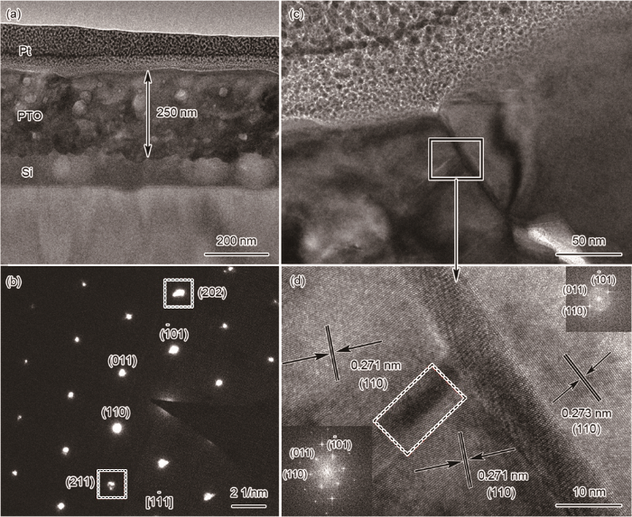
图4
添加0.5%纳米片的PTO薄膜的断面TEM照片及其PTO薄膜的选取电子衍射图(SAED)、两个晶粒晶界区域的TEM照片及其方框区域的高倍TEM照片
Fig.4
Cross-section TEM image of PTO film with 0.5% nanoplates addition (a), Selected area electron diffraction (SAED) patterns of PTO film in (a) (b), Cross-section TEM image of grain boundary area between two grains (c) and High resolution TEM image of the rectangle area in (c) (d)
2.3 PTO薄膜的生长机制
为了深入研究纳米片对PTO薄膜生长机制的影响,对添加含量为0.5%纳米片的PTO前驱体干燥凝胶粉末进行了热分析和红外光谱分析。图5给出了PTO前驱体凝胶粉末的差热和热重曲线,其中253℃的放热峰对应添加剂乙二醇甲醚和乙酰丙酮等挥发性组分的燃烧[28],312℃的放热峰对应聚合物网络结构的燃烧分解[8]。这两个过程的总质量损失为19.44%。451℃的放热峰是PTO的结晶峰,因为在这个温度附近基本上没有质量损失[29]。图6给出了PTO前驱体凝胶粉末在不同温度热处理后的红外谱图,其中在200℃热处理的样品位于3430 cm-1处的峰为-OH基的伸缩振动峰,1545 cm-1处的是-COO基的反对称振动峰,1404 cm-1和1334 cm-1处的是-COO基的对称振动峰[30]。这些基团,来源于制备过程中添加的有机组分乙二醇甲醚和醋酸。在400℃热处理后这些峰消失,表明有机组分完全燃烧挥发。处理温度为450℃时在721 cm-1和577 cm-1处出现两个新的峰并且保持到650℃,这两个峰对应Ti-O八面体伸缩振动的峰[31,32],说明此时薄膜已结晶,与图5中结晶峰对应的温度451℃吻合。
图5
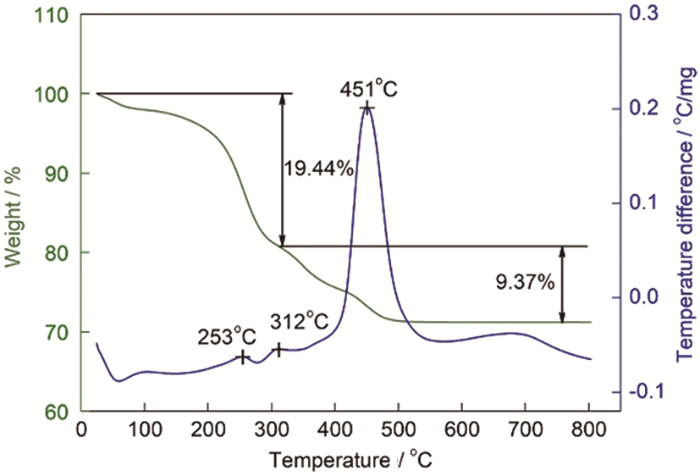
图5
添加0.5%纳米片的PTO前驱体干燥凝胶粉末的DTA和TGA曲线
Fig.5
DTA and TGA curves of PTO precursor gel powder with 0.5% addition of nanoplates
图6
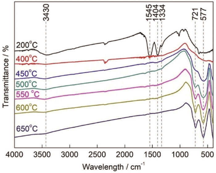
图6
添加0.5%纳米片的PTO前驱体干燥凝胶粉末在不同温度热处理后的FTIR图
Fig.6
FTIR spectra of PTO precursor gel powder with 0.5% addition of nanoplates after heat treatment in different temperatures
进一步对添加0.5%纳米片的PTO前驱体凝胶膜进行了原位升温XRD测试,结果如图7所示。温度由400℃升高到470℃(001)峰向右移动,(100)峰向左移动(图7a),对应晶格常数c减小,a增加,PTO的四方性逐渐减弱,(101)和(110)两个峰也逐渐宽化趋向于合并(图7b)。温度升高到490℃则(001)和(100)以及(101)和(110)的衍射峰合二为一,表明PTO发生了由四方相转变为立方相的相变,晶格常数a和c相等。值得注意的是,图7a中400℃时的(001)峰强度高于(100)峰,但是在450℃和470℃时(100)峰更强。根据TGA和FTIR的结果,400℃时PTO还未结晶,而在纳米片的XRD图谱中(001)峰的衍射强度大于(100)峰[23]。由此可以推断,400℃时XRD的衍射峰来自于纳米片,升温到450℃时PTO已成核结晶且晶粒为(100)取向,因此(001)的衍射峰被压低。
图7
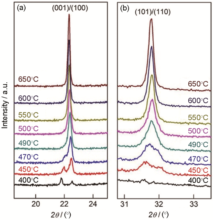
图7
PTO前驱体凝胶膜的原位XRD图谱
Fig.7
In-situ
薄膜的取向与衬底或者添加的中间层的取向一致,例如在[100]MgO和[001]SrTiO3衬底上生长的PbTiO3薄膜的取向分别为(100)和(001)[8],用添加(100)取向的LaNiO3缓冲层制备的PbTiO3薄膜为(100)择优取向[16]。但是在本文制备的PTO薄膜中,(001)为主要暴露面的纳米片诱导了(100)取向的薄膜生长,可能与纳米片的堆积方式有关。在用旋涂法制备薄膜的过程中,纳米片以“平躺”的方式平铺在衬底,能量最低,即(001)面与衬底接触。但是,混合在PTO的溶胶体系中的纳米片受到溶胶的阻力不能产生平铺结构。实际上,在制备出的PTO薄膜中纳米片以“斜插”和“直立”的方式堆积。如图8a所示,对于“斜插”方式(001)和(100)面的暴露均等,而“直立”方式完全暴露(100)面。因此在宏观上,(100)面比(001)面暴露得更多。但是(001)面的面积远大于(100),在XRD图谱中(001)的衍射峰强度更高。而对于PTO的成核结晶,暴露数量更多的(100)面诱导PTO颗粒的(100)取向,最终生成(100)择优取向的薄膜。
图8
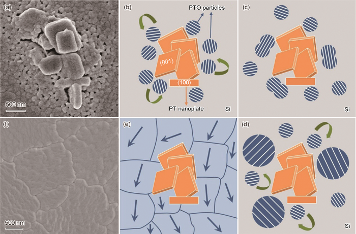
图8
PTO薄膜中纳米片区域的SEM照片、PTO薄膜取向聚集生长四个过程的示意图以及OA生长的最终形貌
Fig.8
SEM image of PTO film areas including nanoplates (a), schematic illustrations of four stages for OA growth (b)~(e) and SEM image of PTO film at the last stage of OA growth (f)
用湿化学方法合成的纳米晶有两种生长机制,分别为OR(Ostwald ripening)生长和OA(Oriented attachment)生长。OR生长即Ostwald熟化过程,在形成固定数量的晶核后大颗粒摄取溶解的小颗粒而长大[33,34]。大颗粒的能量低浓度也低,小颗粒为了释放能量向大颗粒扩散并溶解,使大颗粒不断长大。OR生长由扩散控制,生成的晶体大多是规则的,与材料的晶体结构相关。OA生长即取向聚集生长,是Penn和Banfield等在1998提出的[35,36],指多个取向不同的纳米颗粒旋转使其晶格一致,以初始颗粒作为堆积单元进行定向附着生长,长成大晶体。OA生长可通过静电力、范德华力、表面吸附、电场或磁场等因素控制,晶体形貌不受材料本征晶体结构的限制,其尺寸决定于作为堆积单元的初始颗粒的尺寸 [27]。
根据在PTO薄膜中观察到的晶粒形貌和物相演变可以推断,在PTO结晶后OA生长。根据TGA和FTIR的结果,PTO薄膜在400~450℃开始结晶,在此温度下纳米片仍保持四方铁电性,具有自发极化,因此在两个极化表面产生强静电力,对带电基团有静电吸附作用。研究表明,强表面吸附作用能控制OA机制[37]。PTO薄膜的OA生长过程,如图8b~e所示。首先,纳米片的堆积方式使其极化表面暴露在PTO溶胶凝胶体系中,前驱体粒子定向吸附在纳米片周围成核结晶(图8b)。接着,相邻的晶粒定向旋转使晶向一致且融合长大(图8c)。在此过程中不断有新晶粒形成,重复旋转融合的过程使晶粒不断变大(图8d)。最终,大晶粒边缘变得不规则,使相邻有相近的取向(图8e)的晶粒互相拼接形成薄膜(图8f)。用OA机制能很好地解释图3b和c晶粒中的条状纹路以及在图4d中的红色框区域观察到的现象。
另外,纳米片的横向尺寸为600-1100 nm,而OA生长的晶体尺寸主要由最初始的“堆积单元”决定,因此最终PTO薄膜的晶粒尺寸为1-2 μm。而且纳米片的含量越高表面吸附作用越强,控制OA生长生成的晶粒尺寸越大。如图3所示,加入含量为0.5%的纳米片制备的PTO薄膜其晶粒尺寸明显大于纳米片含量为0.2%的薄膜。但是,纳米片含量提高到0.8%晶粒尺寸却没有明显的变大,因为0.5%含量的PT对应的薄膜晶粒尺寸已达到“堆积单元”纳米片的尺寸,添加0.8%含量纳米片后薄膜晶粒的尺寸饱和,不能继续长大。
3 结论
(1) 将具有自发极化的PTO纳米片加入到溶胶体系中,用溶胶凝胶法可制备出(100)择优取向的PTO薄膜,纳米片含量为0~0.8%的薄膜其晶粒尺寸的调控范围为100 nm~2 μm。
(2) 添加纳米片后在PTO薄膜的晶粒中可观察到取向相近的小晶粒拼接聚合成大晶粒的痕迹,表明PTO的固相薄膜生长表现出类液相的取向聚集生长的特征。
(3) 纳米片在薄膜中表现出“斜插”和“直立”的堆积形貌,暴露出更多数量的(100)晶面诱导了PTO薄膜的(100)取向生长。纳米片的极化表面暴露在溶胶凝胶体系中,其表面静电力驱动了PTO前驱体粒子的定向吸附和成核结晶,小晶粒取向聚集生长,最终的晶粒尺寸决定于堆积单元的纳米片尺寸。
参考文献
PbTiO3-based perovskite ferroelectric and multiferroic thin films
[J].
Ferroelectric thin films, especially PbTiO3-based perovskite thin films which possess robust spontaneous electrical polarization, are widely investigated and applied in various devices. With the advances in synthesis, characterization and calculation techniques, diverse phenomena and properties are uncovered in ferroelectric thin films. Herein some typical PbTiO3-based perovskite thin films through composition control are introduced, which gives more choices with various ferroelectric or other properties. Strain engineering, as well as some other interfacial effects, is also included to show the possibilities of controlling the lattice structure, the electronic structure as well as the domain structure which are closely connected to ferroelectricity. Multiferroic thin films, which could achieve magnetic-field-controlled polarization reversal, expand the novel applications of ferroelectric thin films. Typical and remarkable progress made in the case of multiferroic PbTiO3-based perovskite thin films is discussed here. Critical problems such as leakage current and fatigue hinder the practical use of ferroelectric and multiferroic thin films, and are also included in this article.
Thin-film ferroelectric materials and their applications
[J].
Ferroelectric thin films: review of materials, properties, and applications
[J].
Orienting ferroelectric films
[J].
Role of the PbTiO3 seed layer on the crystallization behavior of PZT thin films
[J].
A discussion on common characteristics of ferroelectricity, high temperature superconductivity and colossal magnetoresistance (CMR) effect
[J].
铁电性、高温超导电性和庞磁电阻(CMR)效应的共性特征探讨
[J].
Crystallization of textured PbTiO3 deposited from gels
[J].
Mechanical-force-induced non-local collective ferroelastic switching in epitaxial lead-titanate thin films
[J].
Giant polarization sustainability in ultrathin ferroelectric films stabilized by charge transfer
[J].
Enhanced electrical resistivity and properties via ion bombardment of ferroelectric thin films
[J].A novel approach to on-demand improvement of electronic properties in complex-oxide ferroelectrics is demonstrated whereby ion bombardment - commonly used in classic semiconductor materials - is applied to the PbTiO3 system. The result is deterministic reduction in leakage currents by 5 orders of magnitude, improved ferroelectric switching, and unprecedented insights into the nature of defects and intergap state evolution in these materials.
Small-strain (100)/(001)-oriented epitaxial PbTiO3 films with film thickness ranging from nano- to micrometer order grown on (100)CaF2 substrates by metal organic chemical vapor deposition
[J].
Suppressed polar distortion with enhanced Curie temperature in in-plane 90o-domain structure of a-axis oriented PbTiO3 Film
[J].
Texture control of PbTiO3 and Pb(Zr,Ti)O3 thin films with TiO2 seeding
[J].
Effect of TiOx seed layer on the texture and electric properties in La and Ca modified PbTiO3 thin films
[J].
Effects of LaNiO3 buffer layers on preferential orientation growth and properties of PbTiO3 thin films
[J].
Growth of highly textured PbTiO3 films on conductive substrate under hydrothermal conditions
[J].
X-ray diffraction study on the grain-size-dependences of orientation and 90o-domain structure in oriented PbTiO3 thin films on (111) Pt
[J].
The effect of grain size on domain structure in unsupported thin films
[J].
Grain size effect on the phase transitions in oriented PbTiO3 thin films deposited by the sol-gel method on (111) Pt/Si
[J].
Electrostatic force-driven oxide heteroepitaxy for interface control
[J].
Polarization-dependent epitaxial growth and photocatalytic performance of ferroelectric oxide heterostructures
[J].
Self-templated synthesis of single-crystal and single-domain ferroelectric nanoplates
[J].
Unit-cell scale mapping of ferroelectricity and tetragonality in epitaxial ultrathin ferroelectric films
[J].Typically, polarization and strain in ferroelectric materials are coupled, leading to the generally accepted direct relation between polarization and unit-cell tetragonality. Here, by means of high-resolution transmission electron microscopy we map, on the unit-cell scale, the degree of tetragonality and the displacements of cations away from the centrosymmetry positions in an ultrathin epitaxial PbZr(0.2)Ti(0.8)O(3) film on a SrRuO(3) electrode layer deposited on a SrTiO(3) substrate. The lattice is highly tetragonal at the centre of the film, whereas it shows reduced tetragonality close to the interfaces. Most strikingly, we find that the maximum off-centre displacements for the central area of the film do not scale with the tetragonality. This challenges the fundamental belief in a strong polarization-tetragonality coupling in PbTiO(3)-based ferroelectrics, at such thicknesses. Furthermore, a systematic reduction of the atomic displacements is measured at the interfaces, suggesting that interface-induced suppression of the ferroelectric polarization plays a critical role in the size effect of nanoscale ferroelectrics.
Structural, dielectric, and ferroelectric properties of PbTiO3 thin films by a simple sol-gel technique
[J].
Progress of nanocrystalline growth kinetics based on oriented attachment
[J].The crystal growth mechanism, kinetics, and microstructure development play a fundamental role in tailoring the materials with controllable sizes and morphologies. The classical crystal growth kinetics-Ostwald ripening (OR) theory is usually used to explain the diffusion-controlled crystal growth process, in which larger particles grow at the expense of smaller particles. In nanoscale systems, another significant mechanism named
Preparation of PbTiO3 by seeding-assisted chemical sol-gel
[J].
Decomposition and crystallization of a sol-gel-derived PbTiO3 precursor
[J].
Crystallization behavior in a low temperature acetate process for perovskite PbTiO3, Pb(Zr,Ti)O3, and (Pb1-x,Lax)(Zry,Ti1-y)1-x/4O3 bulk powders
[J].
Perovskite-structured PbTiO3 thin films grown from a single-source precursor
[J].
Synthesis and structure of nanocrystalline oxides based on PbTiO3 by sol-gel process
[J].
Growth kinetics of grain-boundary precipitates
[J].
Coarsening of Grain-Boundary Precipitates
[J].
Imperfect oriented attachment: dislocation generation in defect-free nanocrystals
[J].Dislocations are common defects in solids, yet all crystals begin as dislocation-free nuclei. The mechanisms by which dislocations form during early growth are poorly understood. When nanocrystalline materials grow by oriented attachment at crystallographically specific surfaces and there is a small misorientation at the interface, dislocations result. Spiral growth at two or more closely spaced screw dislocations provides a mechanism for generating complex polytypic and polymorphic structures. These results are of fundamental importance to understanding crystal growth.
Oriented attachment and growth, twinning, polytypism, and formation of metastable phases; insights from nanocrystalline TiO2
[J].
A multistep oriented attachment kinetics: Coarsening of ZnS nanoparticle in concentrated NaOH
[J].
