
宋瑞利 , 张柯
, 张柯
SONG Ruili, ZHANG Ke
中图分类号: TB331
文章编号: 1005-3093(2016)04-0255-08
通讯作者:
收稿日期: 2015-07-27
修回日期: 2015-08-13
网络出版日期: 2016-04-25
版权声明: 2016 《材料研究学报》编辑部 《材料研究学报》编辑部
基金资助:
展开
摘要
为了制备高质量、少层数的石墨烯薄膜, 分别用25%HCl、2 mol/L FeCl3腐蚀液及电化学抛光法处理铜箔, 改善其表面平整度, 然后利用化学气相沉积法在其表面生长石墨烯。通过调整2 mol/L FeCl3腐蚀铜箔的时间和电化学抛光铜箔的参数, 根据SEM表征结果确定出腐蚀时间为30 s, 抛光电压为10 V, 抛光时间为60 s时, 铜箔表面最为平整。这些方法处理铜箔后生长的石墨烯经拉曼光谱表征后得出, 随着铜箔表面逐渐平整, 铜箔表面更易生长出少层数, 高质量的石墨烯薄膜。实验中还通过调整化学气相沉积(CVD)炉中通乙烯的时间来制备石墨烯。经SEM和拉曼光谱表征可知, 延长生长时间, 石墨烯薄膜的层数变厚, 生长时间过短则石墨烯生长不连续。生长时间为30 s时, 可生长出单层高质量的石墨烯薄膜, 且石墨烯薄膜均匀致密; 生长时间为60 s时, 铜箔表面沉积一层石墨。所以生长单层石墨烯, 控制生长时间是必要的。
关键词:
Abstract
High-quality and few-layered graphene was grown by chemical vapor deposition (CVD) on copper foils, which were pre-treated by etching with 25%HCl or 2 mol/L FeCl3 and then electrochemical polishing in order to improve their surface smoothness. The surface morphology of the copper foils and the deposited graphene were characterized by means of Raman spectroscopy, XRD and SEM etc. The results showed that copper foils with desired surface smoothness would be acquired through etching with 2 mol/L FeCl3 for 30 s and then electrochemical polishing for 60 s by applied voltage of 10 V; Films of layered graphene with less defects could be deposited on the pre-treated copper foils. The thickness of graphene films increased with the increasing time, however for a short deposition time the formed graphene films were discontinuous with poor quality. The monolayered high-quality graphene films could be prepared by depositing for 30 s, whilst the deposition time increased to 60 s a graphite film could form on the surface. In other word, it is necessary to control the deposition on time for growing the desired monolayered graphene films.
Keywords:
石墨烯是一种sp2杂化碳原子堆积成的二维蜂窝状六边形晶格[1], 具有高导电[2]、高存储[3]及良好的光学透过率[4]等性能。自从2004年Novoselov等[5]采用机械剥离法制备出石墨烯后, 这种明星材料引起了很多研究者的兴趣。虽然机械剥离法能够制备出稳定存在的石墨烯, 但是该方法制备出的石墨烯的面积较小。研究者们尝试出其它制备石墨烯的方法, 其中化学气相沉积法(CVD法)利用金属做基底可以制备出高质量大面积的石墨烯[2, 6-8]。用铜[9-16]金属做衬底, 制备成本比较低。近年来, 提高铜上生长石墨烯的质量成为了研究热点, 其中多数集中于对生长参数、控制成核位置等的研究, 并取得了一定成果[17-19]。铜箔表面处理[20-23]对石墨烯质量的影响的研究比较少。石墨烯的生长可以越过铜表面的各种微观形貌(台阶、凹坑等)及大部分的缺陷(位错、原子突起等[24, 25]), 甚至于非晶区域[26]。但铜粗糙的表面结构依然会对其上生长的石墨烯的质量产生一些不良的影响:铜表面的台阶状结构可能会使石墨烯的晶向发生偏转, 从而形成晶界等缺陷[27]; 石墨烯倾向于在缺陷和微观结构粗糙处成核, 增大成核密度等。因此, 铜表面形貌和质量很大程度上决定了所制备石墨烯的质量。目前有研究者利用盐溶液[28]、电化学抛光[29, 30]等方法对铜箔表面处理, 这些方法都一定程度的提高了石墨烯的质量。
本研究对铜箔处理工艺进行着重探讨, 分别利用酸、盐溶液和电化学抛光的方法处理铜箔, 通过调整工艺参数, 利用SEM和拉曼光谱仪测试表征, 设计出一种最佳的铜箔处理工艺。本文还探讨了生长时间对制备石墨烯的影响。
压延铜箔(纯度为99.9%), 乙醇(分析纯 AR), 丙酮(分析纯 AR), 去离子水(自制), 盐酸(分析纯 AR, HCl含量36.0%~38.0%), 氯化高铁(分析纯 AR, FeCl36H2O), 磷酸(优级纯 GR), 异丙醇(分析纯 AR), 尿素(分析纯 AR), 乙烯(C2H4, 纯度≥99.7%), 高纯氩气(Ar, 纯度≥99.999%)、氢气(H2, 纯度≥99.999%)、聚甲基丙烯酸甲酯(PMMA), 苯甲醚(化学纯 CP), Si/SiO2(规格为20 mm×20 mm×3 mm)等。
用KQ3200DE型数控超声波清洗机将尺寸为20 mm×20 mm×0.03 mm的压延铜箔分别在丙酮、乙醇、去离子水中超声清洗10 min, 然后用25%的盐酸超声清洗10 min, 最后用去离子水超声清洗铜箔5 min三次。
分别用丙酮, 乙醇, 去离子水超声清洗20 mm×20 mm×0.03 mm大小的压延铜箔10 min, 然后用2 mol/L的FeCl3溶液静置清洗铜箔一定时间, 然后用去离子水超声清洗铜箔5 min三次, 再用去离子水清洗该铜箔5 min三次。
本实验中把用稀盐酸处理后的铜箔进行抛光。所用的电化学抛光电源为CHI660d型电化学工作站, 抛光电压为10 V, 抛光时间分别为80, 60, 40, 20 s, 灵敏度为1.0×e-1, 抛光液的配比为去离子水∶磷酸∶乙醇∶异丙醇∶尿素=100 mL∶50 mL∶50 mL∶10 mL∶1 g, 阳极接工作电极(铜箔), 阴极接0.3 mm的铜板。
将处理好的铜箔放在石英板上, 然后放入OTF-1200X型CVD管式炉的恒温处, 在氩气流量为3000 mL/min和氢气流量为300 mL/min氛围下升温至950℃, 然后保温60 min得到表面质量更高的铜箔。之后通入乙烯氩气混合气体(n(C2H4)∶n(Ar)=1∶9)流量调为10 mL/min, 时间分别为15, 30, 45 s。
为了更好地表征和测试石墨烯, 采用腐蚀基底法[31]把石墨烯转移到SiO2/Si基底上, 利用KW-4A型台式匀胶机将PMMA均匀旋涂于石墨烯/铜箔表面, PMMA薄膜干燥后放入2 mol/L FeCl3腐蚀液中腐蚀12 h以去除铜箔。用去离子水冲洗PMMA/Graphene薄膜3次, PMMA/Graphene薄膜转移到SiO2/Si基底上, 待PMMA/Graphene薄膜固定在SiO2/Si基底上后, 将PMMA/Graphene/SiO2/Si放入丙酮溶液中静置2 d, 更换新的丙酮溶液, 再将样品放入其中静置3 h, 然后用去离子水缓慢清洗样品3次, 去除PMMA, 得到Graphene/SiO2/Si样品。
利用D8-Advanced Bruker AVS型X射线衍射仪(XRD)测试退火前铜箔的物相; 利用FEI Quanta 450型场发射扫描电子显微镜(SEM)观察铜箔表面形貌; 利用HR Evolution型拉曼光谱仪测试铜箔表面生长的石墨烯的拉曼图谱, 激光波长为532 nm。
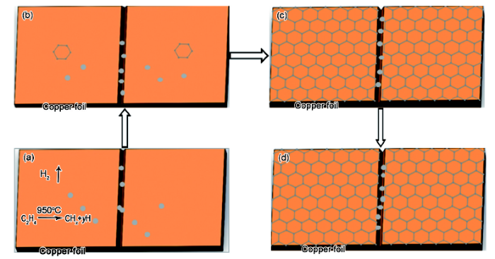
图1为石墨烯在不平整铜箔表面生长时的生长机理模型图, 图中央的凹槽部分为铜箔表面不平整处的示意图, 石墨烯在铜箔表面形成过程大致是由3个步骤: (1) C2H4在950oC高温下的铜箔表面分解, 最终分解成H2和C, 然后碳附着在铜箔表面; (2) 石墨烯开始成核和长大; (3) 反应终止。从这四张图可以清晰的看出在铜箔不平整处没有形成完整的石墨烯。在开始阶段, 乙烯在高温条件下吸附在铜箔表面, H原子从乙烯分子中分离出来, 在平整的铜箔晶粒和不平整(台阶, 压延痕迹等)的铜箔表面产生活性碳。在生长的整个过程中, 乙烯分离出的H原子重组形成氢气分子。碳分散在铜表面, 形成多环烃结构, 最后形成石墨烯薄膜。活性碳在平整的铜箔表面能够形成石墨的sp2杂化的网状结构。然而在铜箔的不平整表面, 活性碳被困在铜箔表面的“山谷”里面, 缺乏形成大规模石墨烯的表面迁移的环境, 从而导致缺陷的形成, sp2网状结构的终止。最后在不平整铜箔表面形成石墨烯碎片或无定形碳, 如图1d的不平整处的灰色圆圈。所以在制备高质量的石墨烯之前, 铜箔表面的平整是十分重要的。
图1 石墨烯在不平整铜箔表面生长时的生长机理模型图
Fig.1 Model diagram of graphene growth mechanism on rough copper foil surface, (a) dissociation of hydrocarbon on heated copper foil surface, (b) nucleation and growth of graphene, (c) reaction termination, (d) final graphene and final amorphous carbon on the rough surface of copper foil
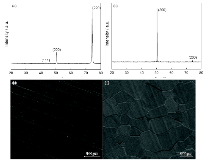
图2a和c为铜箔退火前的XRD图和铜箔表面的SEM图, 图2b和d为铜箔退火后的XRD图和铜箔表面的SEM图, 退火温度为950oC, 退火时间为60 min。可以看到, 退火前铜箔存在(111)、(200)和(220)三个衍射峰, 铜箔表面形貌存在明显的条形压延痕迹, 而退火后的铜箔产生晶粒取向, 对应的XRD图只出现了一个(200)的窄峰和一个很矮的(220)面, 铜箔表面出现大的铜晶粒, 明显比退火前的铜箔表面平整。
图2 铜箔退火前后的XRD和SEM表征图
Fig.2 XRD and SEM characterization of copper foils before and after annealing, (a) copper foils before annealing, (b) copper foils after annealing, (c) copper foils before annealing, (d) copper foils after annealing
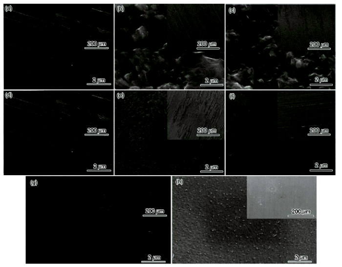
图3为不同条件下处理铜箔的SEM图。图3a为25%HCl清洗10 min铜箔的SEM图, 可见铜箔表面有明显的原始加工工艺留下的压延条形痕迹。图3b、c和d为2 mol/L FeCl3溶液腐蚀15, 30, 45 s铜箔的SEM图, 从低倍SEM图可以看出, 与图3a相比, 经FeCl3溶液腐蚀的铜箔压延痕迹变浅, 铜箔表面平整度得到改善, 其中图3c条件下的铜箔表面平整度最好, 所以2 mol/L FeCl3溶液腐蚀铜箔的时间为30 s时, 铜箔表面平整度最好; 时间为15 s时, 时间不足; 时间为45 s时, 铜箔腐蚀过度。图3e、f、g和h为电化学抛光铜箔的SEM图, 抛光电压为10 V, 抛光时间分别为20, 40, 60, 80 s, 可以明显看到这四种条件对应的铜箔表面平整度均比图3a-d对应腐蚀条件的铜箔表面好, 其中图3g对应条件的铜箔表面最平整, 所以电化学抛光铜箔的工艺参数为10 V、60 s时最佳。
图3 不同处理条件下的铜箔的表面形貌
Fig.3 SEM images of copper foils treated by different processing conditions, (a)washed by 25% HCl for 10 min, (b) to (d) etched by 2 mol/L FeCl3 for 15 s, 30 s and 45 s respectively, (e) to (g) electrochemically polished at 10 voltage for 20 s, 40 s, 60 s and 80 s respectively
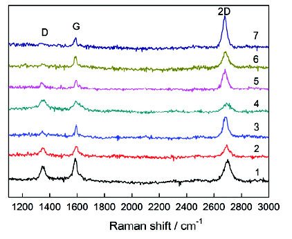
拉曼光谱可以用来确定石墨烯的层数和取向, 质量和边缘类型, 和扰动的影响, 如电场和磁场、应变、掺杂、混乱和官能团。激光激发引起斯托克斯声子能量的转变产生3个主要的拉曼峰: 一个主平面振动模式的峰G(1580 cm-1)峰, 以及一个不同的面内振动的二阶泛音的2D峰(2690 cm-1), 还有一个D(1350 cm-1)峰。利用ID/IG比值可以判断出石墨烯的质量和无序性, I2D/IG比值判断石墨烯的层数, 2D峰的半高宽可以进一步判断石墨烯的层数[32]。图4为在不同处理条件下的铜箔表面生长的石墨烯后转移到SiO2/Si基底的拉曼光谱图。图中铜箔的处理条件分别是用25%HCl、2 mol/L FeCl3溶液腐蚀及电化学抛光, 然后在950℃下退火2 h后生长的石墨烯, 生长时间为30 s。表1为图4曲线对应的处理条件和生长的石墨烯对应的拉曼光谱测试数据, 表1中很清楚的看出及可以清楚的对比出铜箔经过7种前处理后生长的石墨烯的拉曼数据ID/IG、I2D/IG以及半高宽的值。图4中的曲线1是由25%HCl腐蚀液清洗10 min铜箔表面生长的石墨烯的拉曼图谱, 从图中可以看出该曲线的D峰的强度很高。图4的曲线2、3和4是由2 mol/L FeCl3腐蚀铜箔时间分别为15, 30, 45 s后生长的石墨烯的拉曼图谱。图4的曲线5、6和7是由10 V电压下电化学抛光的铜箔时间分别为20, 40, 60 s后生长的石墨烯的拉曼光谱图, 其中10 V、80 s铜箔表面腐蚀过度不做讨论。
图4 不同处理条件下的铜箔表面生长的石墨烯的拉曼表征图
Fig.4 Raman characterization of graphene on copper foils treated by different conditions
表1 不同处理条件下的铜箔表面生长的石墨烯的拉曼数据
Table 1 Raman data of graphene on copper foils treated by different conditions
| Curve number of Fig.4 | Treatment condition | ID/IG | I2D/IG | Full width at half maximum (cm-1) |
|---|---|---|---|---|
| 1 | 25%HCl, 10 min | 0.67 | 0.93 | 57 |
| 2 | 2 mol/L FeCl3, 15 s | 0.57 | 1.14 | 40 |
| 3 | 2 mol/L FeCl3, 30 s | 0.51 | 1.71 | 39 |
| 4 | 2 mol/L FeCl3, 45 s | 1.14 | 0.86 | 47 |
| 5 | Polished 30 s | 0.6 | 2.6 | 35.5 |
| 6 | Polished 45 s | 0.42 | 1.38 | 47 |
| 7 | Polished 60 s | 0.4 | 1.63 | 44 |
综上描述, 依据图2、图4和表1的数据和分析可知, 随着铜箔表面平整度变好, 这些曲线对应的ID/IG比值变小, 缺陷变少, I2D/IG值变大, 2D峰的半高宽变窄, 生长出的石墨烯的质量变好, 更易生长出少层数的石墨烯。
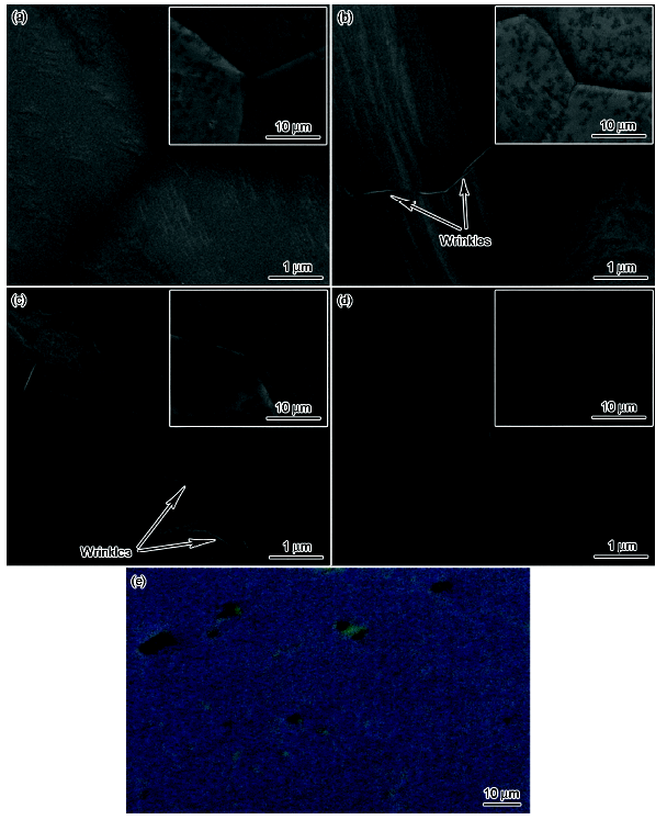
图5为在10 V、60 s电化学抛光铜箔的表面生长石墨烯的表征图。图5a-d生长时间为15, 30, 45, 60 s的石墨烯的SEM图。从图5a可以看出有石墨烯的存在, 但没有褶皱的出现, 在晶界处也没有出现褶皱。从图5b可以看出有褶皱的出现, 图中箭头指的位置为褶皱, 而且该褶皱跨过了铜箔的晶界, 说明该条件下生长的石墨烯在铜箔表面是连续的, 图5e为对应转移到SiO2/Si基底上的偏光显微镜, 可以清楚地看到石墨烯的形貌, 因为石墨烯转移到SiO2/Si基底上, 是属于原位转移, 所以石墨烯转移后的结构特点不会改变。从图5c可以看出有褶皱的出现, 箭头的指向为褶皱, 而且褶皱比较多, 该条件下生长的石墨烯也是连续的。从图5d中可以看出有一层比较大的黑色区域。
图5 10 V 60 s电化学抛光铜箔表面生长的石墨烯的表征图
Fig.5 SEM characterization of graphene grown on copper foils electrochemically polished at 10 V for 60 s, (a) to (d) graphene growth time of 15 s, 30 s, 45 s and 60 s, (e) polarizing microscope imagines of graphene growth time of 30 s
综上可知, 随着生长时间的增加, 在铜箔表面沉积的黑色区域是越来越多, 石墨烯生长越来越厚。生长时间为30 s和45 s时, 有通过铜箔晶界的褶皱出现, 可以生长出比较连续的石墨烯。
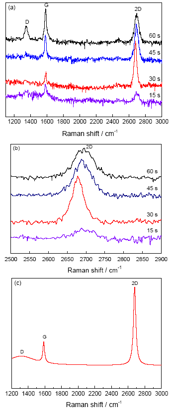
图6为在10 V、 60 s电化学抛光铜箔的表面生长石墨烯的Raman光谱图。从图6a中的生长时间为15 s的石墨烯的Raman图中分析, 在石墨烯样品上取4个点, 其中就有一个点有峰的存在, 对应的ID/IG=0.4, I2D/IG=1, 半高宽=35 cm-1, 2D峰的波数为2692 cm-1, 说明该条件下生长的石墨烯不连续。图6a中的生长时间为30 s的石墨烯的Raman图中分析, 对应的ID/IG=0.38, I2D/IG=4, 半高宽=33 cm-1, 2D峰的波数为2678.32 cm-1均说明该条件下的石墨烯为单层石墨烯, 图6c为图6a中生长时间为30 s的拉曼光谱图的洛伦兹函数拟合曲线, 该拟合曲线的2D峰是单峰以及对称峰, 进一步说明该条件下的石墨烯的单层性。图6a中的生长时间为45 s的石墨烯的Raman图中分析, 对应的ID/IG=0.4, I2D/IG=1.42, 半高宽=43 cm-1, 2D峰的波数为2687.7 cm-1。图6a中的生长时间为60 s的石墨烯的Raman图中分析, 对应的ID/IG=0.5, I2D/IG=0.9, 半高宽=58.81 cm-1, 2D峰的波数为2695.62 cm-1, 说明该条件下生长出的为石墨。图6b为图6a对应的2D峰放大图, 从图中的2D峰的位置很明显发现, 随着生长时间的增加, 2D峰的峰位发生了蓝移。
图6 10 V 60 s电化学抛光铜箔表面生长的石墨烯的Raman图
Fig.6 Raman spectra of graphene grown on copper foils electrochemically polished at 10 V for 60 s, (a) graphene of growth time of 15 s, 30 s, 45 s and 60 s (transferred to SiO2/Si substrate), (b) 2D peak corresponding to Fig.a, (c) curve fitted by the Lorenz function of growth time of 30 s of Fig.a
综上可知, 生长时间为30 s至60 s, 拉曼数据的I2D/IG值变小, 2D峰的半高宽变宽, 说明石墨烯的层数逐渐增多, 这与之前说的随着时间增加, 2D峰发生蓝移吻合。ID/IG值变大, D峰升高, 这是由于铜箔表面的石墨烯岛逐渐增多, 从而石墨烯的边界也变多, 则D峰就会升高。电化学抛光电压10 V, 腐蚀时间60 s, 生长时间为30 s时可以生长出高质量单层的石墨烯。
1. 电化学抛光铜箔在10 V电压下, 随着时间的增加, 铜箔的平整度变好, 其中60 s最佳, 时间过长, 铜箔会被抛光过度。
2. 石墨烯的拉曼光谱分析表明, 随着铜箔表面的质量变好, ID/IG比值变小, I2D/IG比值变大, 半高宽变小, 生长出石墨烯层数少、缺陷小。随着生长时间的增加, I2D/IG比值变小, 半高宽变大, 石墨烯的层数变多。
3. 电化学抛光铜箔的参数为10 V、时间60 s, 石墨烯生长时间30 s的条件下的制备的石墨烯的ID/IG=0.38, I2D/IG=4, 半高宽=33 cm-1, 表明该条件下可以生长出少层数高质量的石墨烯。
The authors have declared that no competing interests exist.
| [1] |
The rise of graphene , |
| [2] |
Roll-to-roll Production of 30-inch Graphene Films for Transparent Electrodes ,
The outstanding electrical, mechanical and chemical properties of graphene make it attractive for applications in flexible electronics. However, efforts to make transparent conducting films from graphene have been hampered by the lack of efficient methods for the synthesis, transfer and doping of graphene at the scale and quality required for applications. Here, we report the roll-to-roll production and wet-chemical doping of predominantly monolayer 30-inch graphene films grown by chemical vapour deposition onto flexible copper substrates. The films have sheet resistances as low as ~125 Ω□with 97.4% optical transmittance, and exhibit the half-integer quantum Hall effect, indicating their high quality. We further use layer-by-layer stacking to fabricate a doped four-layer film and measure its sheet resistance at values as low as ~30 Ω□at ~90% transparency, which is superior to commercial transparent electrodes such as indium tin oxides. Graphene electrodes were incorporated into a fully functional touch-screen panel device capable of withstanding high strain.
|
| [3] |
Graphene-based ultracapacitors , |
| [4] |
Transparent conductive graphene films prepared by hydroiodic acid and thermal reduction ,
Transparent conductive graphene films are fabricated by the transfer printing of graphene aqueous dispersion followed by hydrohalic acids and thermal reduction. Results indicate that the graphene film reduced by hydroiodic acid (HI) reduction combined with thermal treatment shows a higher electrical conductivity than that reduced only by thermal treatment at the same transparency. A film with a sheet resistance of ~ 2400 惟/sq at a transparency over 72% is obtained at a typical wavelength of 550 nm.
|
| [5] |
Electric field effect in atomically thin carbon films ,
We describe monocrystalline graphitic films, which are a few atoms thick but are nonetheless stable under ambient conditions, metallic, and of remarkably high quality. The films are found to be a two-dimensional semimetal with a tiny overlap between valence and conductance bands, and they exhibit a strong ambipolar electric field effect such that electrons and holes in concentrations up to 10(13) per square centimeter and with room-temperature mobilities of approximately 10,000 square centimeters per volt-second can be induced by applying gate voltage.
|
| [6] |
Research on synthesis of high-quality and large-scale graphene films by chemical vapor deposition ,高质量大面积石墨烯的化学气相沉积制备方法研究 ,
石墨烯因其奇特的能带结构和优异的物理性能而成为近年来大家研究的热点, 但是目前单层石墨烯的质量与尺寸制约了其实际应用的发展. 本文采用常压化学气相沉积(CVD)方法, 基于铜箔衬底, 利用甲烷作为碳源制备了高质量大面积的单层与多层石墨烯. 研究发现: 高温度、稀薄的甲烷浓度、较短的生长时间以及合适的气体流速是制备高质量、大面积石墨烯的关键. Raman光谱, 扫描电子显微镜、透射电子显微镜等表征结果表明: 制备的石墨烯主要为单层, 仅铜箔晶界处有少量多层石墨烯. 电学测试表明CVD制备的石墨烯在低温时呈现出较明显的类半导体特性; 薄膜电阻随外界磁场的增大而减小.
|
| [7] |
Repeated growth and bubbling transfer of graphene with millimetre-size single-crystal grains using platinum ,
Large single-crystal graphene is highly desired and important for the applications of graphene in electronics, as grain boundaries between graphene grains markedly degrade its quality and properties. Here we report the growth of millimetre-sized hexagonal single-crystal graphene and graphene films joined from such grains on Pt by ambient-pressure chemical vapour deposition. We report a bubbling method to transfer these single graphene grains and graphene films to arbitrary substrate, which is nondestructive not only to graphene, but also to the Pt substrates. The Pt substrates can be repeatedly used for graphene growth. The graphene shows high crystal quality with the reported lowest wrinkle height of 0.8 nm and a carrier mobility of greater than 7,100 cm(2) V-1 s(-1) under ambient conditions. The repeatable growth of graphene with large single-crystal grains on Pt and its nondestructive transfer may enable various applications.
|
| [8] |
Large-scale pattern growth of graphene films for stretchable transparent electrodes ,
Problems associated with large-scale pattern growth of graphene constitute one of the main obstacles to using this material in device applications. Recently, macroscopic-scale graphene films were prepared by two-dimensional assembly of graphene sheets chemically derived from graphite crystals and graphene oxides. However, the sheet resistance of these films was found to be much larger than theoretically expected values. Here we report the direct synthesis of large-scale graphene films using chemical vapour deposition on thin nickel layers, and present two different methods of patterning the films and transferring them to arbitrary substrates. The transferred graphene films show very low sheet resistance of approximately 280 Omega per square, with approximately 80 per cent optical transparency. At low temperatures, the monolayers transferred to silicon dioxide substrates show electron mobility greater than 3,700 cm(2) V(-1) s(-1) and exhibit the half-integer quantum Hall effect, implying that the quality of graphene grown by chemical vapour deposition is as high as mechanically cleaved graphene. Employing the outstanding mechanical properties of graphene, we also demonstrate the macroscopic use of these highly conducting and transparent electrodes in flexible, stretchable, foldable electronics.
|
| [9] |
Growth of adlayergraphene on Cu studied by carbon isotope labeling ,
The growth of bilayer and multilayer graphene on copper foils was studied by isotopic labeling of the methane precursor. Isotope-labeled graphene films were characterized by micro-Raman mapping and time-of-flight secondary ion mass spectrometry. Our investigation shows that during growth at high temperature, the adlayers formed simultaneously and beneath the top, continuous layer of graphene and the Cu substrate. Additionally, the adlayers share the same nucleation center and all adlayers nucleating in one place have the same edge termination. These results suggest that adlayer growth proceeds by catalytic decomposition of methane (or CHx, x < 4) trapped in a "nano-chemical vapor deposition" chamber between the first layer and the substrate. On the basis of these results, submillimeter bilayer graphene was synthesized by applying a much lower growth rate.
|
| [10] |
Large-area synthesis of high-quality and uniform graphene films on copper foils , |
| [11] |
Effect of catalyst morphology on the quality of CVD grown graphene ,
ABSTRACT
|
| [12] |
Research progress in preparation and characterization graphene ,
石墨烯的制备与表征研究 ,
石墨烯材料是近两年的一个研究热点.简要回顾了石墨分离的历史,着重介绍了石墨烯的制备方法:GICs插层法、还原氧化石墨法、微机械剥离法和化学沉积法,分析了各种制备方法的特点以及所面临的问题,概述了石墨烯的不同表征方法以及应用,并展望了其未来发展前景.
|
| [13] |
Preparation of graphene by chemical vapor deposition ,石墨烯的化学气相沉积法制备 ,Magsci 摘要
<p><span style="line-height: 150%; font-size: 9pt">化学气相沉积(CVD)法是近年来发展起来的制备石墨烯的新方法,具有产物质量高、生长面积大等优点,逐渐成为制备高质量石墨烯的主要方法。通过简要分析石墨烯的几种主要制备方法(胶带剥离法、化学剥离法、SiC外延生长法和CVD方法)的原理和特点,重点从结构控制、质量提高以及大面积生长等方面评述了CVD法制备石墨烯及其转移技术的研究进展,并展望了未来CVD法制备石墨烯的可能发展方向,如大面积单晶石墨烯、石墨烯带和石墨烯宏观体的制备与无损转移等。</span></p>
|
| [14] |
Overview of the production process on rolled copper foil ,
压延铜箔生产工艺概述 ,
综述了国内外压延铜箔的生产现状,分析了压延铜箔的生产工艺和关 键技术,指出厚度控制、表面质量和表面处理是铜箔生产的关键环节,全面、全过程和全员参与的质量管理制度是压延铜箔生产的保证;介绍了电子铜箔的种类、应 用领域和工业标准;综合对比了电解铜箔与压延铜箔的性能,与电解铜箔相比,压延铜箔具有更好的延伸性和耐折性,更高的软化温度和强度,更低的表面粗糙度, 指出压延铜箔是制造挠性印刷线路板基板的关键材料.
|
| [15] |
Technological analysis of nonferrous metal strip produced by steckel mills ,
炉卷轧机应用于有色金属板带材生产工艺分析 ,
利用炉卷轧机生产有色金属板带 材具有易于在线控温、投资及生产成本低等显著特点.通过对应用在钢铁行业炉卷轧机生产技术、工艺设备特点的分析总结,结合有色金属板带材生产工艺的特点和 需求,重点对钛、镁、铜及其合金板带材利用炉卷轧机热温轧制工艺技术和生产线配置进行了分析."1+1"双机架形式的专用炉卷轧机是可以用来生产钛、镁及 其合金板带材的合适生产线.
|
| [16] |
Copper strip slitting defect analysis and quality control ,铜带材纵剪缺陷分析及质量控制 ,
阐述了圆盘剪的内部结构和剪切功能,分析了铜带材裁剪和分切过程中常见的质量缺陷,提出了改善措施.在实际加工过程中,通过对刀刃侧间隙和重叠量的调节,刀具和刀垫的合理选配及生产现场的品质控制与规范操作,主要缺陷可以得到有效克服,产品质量可控,质量水平能更好地满足用户需求,同时也可以提高工序成材率,获取更多的效益。
|
| [17] |
Colombo Luigi, S. Ruoff Rodney, Large-area graphene single crystals grown by low-pressure chemical vapor deposition of methane on copper ,
Graphene single crystals with dimensions of up to 0.5 mm on a side were grown by low-pressure chemical vapor deposition in copper-foil enclosures using methane as a precursor. Low-energy electron microscopy analysis showed that the large graphene domains had a single crystallographic orientation, with an occasional domain having two orientations. Raman spectroscopy revealed the graphene single crystals to be uniform monolayers with a low D-band intensity. The electron mobility of graphene films extracted from field-effect transistor measurements was found to be higher than 4000 cm(2) V(-1) s(-1) at room temperature.
|
| [18] |
Controllable synthesis of submillimeter single-crystal monolayer graphene domains on copper foils by suppressing nucleation , |
| [19] |
Triggering the continuous growth of graphene toward millimeter-sized grains ,
<p>A simple but efficient strategy to synthesize millimeter-sized graphene single crystal grains by regulating the supply of reactants in the chemical vapor deposition (CVD) process is demonstrated. Polystyrene is used as a carbon source. Pulse heating on the carbon source is utilized to minimize the nucleation density of graphene on copper foil, while a gradual increase in the temperature of the carbon source and the flow rate of hydrogen is adapted to drive the continuous growth of the graphene grains. As a result, the nucleation density of graphene grain can be controlled to as low as ≈100 nuclei/cm<sup>2</sup>, and a single crystal grain can grow up to dimensions of ≈1.2 mm. Raman spectroscopy, transmission electron microscopy (TEM), and electrical-transport measurements show that the graphene grains obtained are of high quality. The strategy presented provides very good controllability and enables the possibility of large graphene single crystals, which is of vital importance for practical applications.</p>
|
| [20] |
Influence of copper morphology in forming nucleation seeds for graphene growth ,
Not Available
|
| [21] |
Brian D’Urso, Chemical vapor deposition of graphene on large-domain ultra-flat copper , |
| [22] |
Significant enhancement of the electrical transport properties of graphene films by controlling the surface roughness of Cu foils before and during chemical vapor deposition , |
| [23] |
Ultrasmooth metallic foils for growth of high-quality graphene by chemical vapor deposition , |
| [24] |
Continuity of graphene on polycrystalline copper ,
Not Available
|
| [25] |
Atomic-scale characterization of graphene grown on copper (100) single crystals ,
Growth of graphene on copper (100) single crystals by chemical vapor deposition has been accomplished. The atomic structure of the graphene overlayer was studied using scanning tunneling microscopy. A detailed analysis of moire superstructures present in the graphene topography reveals that growth occurs in a variety of orientations over the square atomic lattice of the copper surface. Transmission electron microscopy was used to elucidate the crystallinity of the grown graphene. Pristine, defect-free graphene was observed over copper steps, corners, and screw dislocations. Distinct protrusions, known as "flower" structures, were observed on flat terraces, which are attributed to carbon structures that depart from the characteristic honeycomb lattice. Continuous graphene growth also occurs over copper adatoms and atomic vacancies present at the single-crystal surface. The copper atom mobility within vacancy islands covered with suspended graphene sheets reveals a weak graphene substrate interaction. The observed continuity and room-temperature vacancy motion indicates that copper mobility likely plays a significant role in the mechanism of sheet extension on copper substrates. Lastly, these results suggest that the quality of graphene grown on copper substrates is ultimately limited by nucleation at the surface of the metal catalyst.
|
| [26] |
Defect-like structures of graphene on copper foils for strain relief investigated by high-resolution scanning tunneling microscopy ,
Understanding of the continuity and the microscopic structure of as-grown graphene on Cu foils through the chemical vapor deposition (CVD) method is of fundamental significance for optimizing the growth parameters toward high-quality graphene. Because of the corrugated nature of the Cu foil surface, few experimental efforts on this issue have been made so far. We present here a high-resolution scanning tunneling microscopy (STM) study of CVD graphene directly on Cu foils. Our work indicates that graphene can be grown with a perfect continuity extending over both crystalline and noncrystalline regions, highly suggestive of weak graphene-substrate interactions. Due to thermal expansion mismatch, defect-like wrinkles and ripples tend to evolve either along the boundaries of crystalline terraces or on noncrystalline areas for strain relief. Furthermore, the strain effect arising from the conforming of perfect two-dimensional graphene to the highly corrugated surface of Cu foils is found to induce local bonding configuration change of carbon from sp(2) to sp(3), evidenced by the formation of "three-for-six" lattices.
|
| [27] |
Origin of the mosaicity in graphene grown on Cu(111) , |
| [28] |
Study on fabrication parameter of graphene on copper by CVD ,铜基石墨烯的CVD法制备工艺参数研究 ,
采用乙炔作为碳源,分析了碳源 浓度、生长时间等参数对铜基石墨烯成核密度、生长速率及单层覆盖率的影响,通过热氧化法系统展示了石墨烯形核、长大、生长结束的全过程.研究发现;碳源浓 度较小时成核密度较低,所得石墨烯晶粒更大,但单个多层点的面积较大,且多以双层为主;在石墨烯生长过程中,氢气既可辅助碳氢化合物分解,同时也会刻蚀部 分成核点,从而促进石墨烯质量的提高;基于单层率与晶粒尺寸之间的平衡,采用乙炔与氢氩混合气(体积比为1∶9)流速比为5∶100作为生长石墨烯的气体 工艺参数,获得了透过率约为97.1%,缺陷较少且以单层为主的大面积石墨烯.
|
| [29] |
Studies on electrochemical polishing of stainless steel ,
Functions of the components in electrochemical polishing solutions for stainless steel were studied. The effect of operating conditions on polishing results was studied. Bright and level stainless steel surface can be obtained quickly under low current densities at medium temperature.
|
| [30] |
Development of electrochemical polishing technology ,
With development of surface processing,the requirement of surface polishing for precision becomes higher and higher.Traditional technology of surface polishing can hardly satisfy the actual need for precision.Electrochemical polishing(EP) technology has been quickly developed in the field of surface polishing.Compared with traditional polishing technology,the EP technology has some advantages: high efficiency,without damage and internal stresses,lower roughness,hardness of materials unrestrained and so on.The principle and characteristics of EP technology were introduced and the effect of EP was presented.The new development of EP technology was extensively reviewed.
|
| [31] |
Large area, few-layer graphene films on arbitrary substrates by chemical vapor deposition ,
Abstract In this work we present a low cost and scalable technique, via ambient pressure chemical vapor deposition (CVD) on polycrystalline Ni films, to fabricate large area ( approximately cm2) films of single- to few-layer graphene and to transfer the films to nonspecific substrates. These films consist of regions of 1 to approximately 12 graphene layers. Single- or bilayer regions can be up to 20 mum in lateral size. The films are continuous over the entire area and can be patterned lithographically or by prepatterning the underlying Ni film. The transparency, conductivity, and ambipolar transfer characteristics of the films suggest their potential as another materials candidate for electronics and opto-electronic applications.
|
| [32] |
Raman spectroscopy in graphene, Phys ., |

/
| 〈 |
|
〉 |