
陈锋 , 何鑫
, 何鑫
CHEN Feng, HE Xin
中图分类号: TB321
文章编号: 1005-3093(2016)05-0388-05
通讯作者:
收稿日期: 2015-01-25
网络出版日期: 2016-05-25
版权声明: 2016 《材料研究学报》编辑部 《材料研究学报》编辑部
基金资助:
展开
摘要
使用荧光粉和硅胶制备荧光膜, 然后与455 nm蓝光芯片模组组装成高功率的白光LED器件。采用吸收光谱、荧光光谱和电致发射光谱等对荧光膜和器件进行表征, 研究了红色荧光粉与黄色荧光粉的比例对器件性能的影响。结果表明:所制备的荧光膜表面平整、荧光粉分散均匀。Y3Al5O12: Ce3+ (YAG)荧光膜的吸收光谱峰分别位于337 nm和450 nm左右, 与YAG荧光粉中Ce3+的f-d跃迁吸收对应, 且当荧光膜厚度为1.00 mm时制备出的功率为2.8 W左右的LED模组光色参数较好。将不同比例红色荧光粉和黄色荧光粉按上述厚度和条件制备高显色荧光膜和低色温4460 K、高显色指数91.7的白光LED器件。
关键词:
Abstract
The fluorescent films were produced by phosphors and silicones for LED packaging modules. Then the high-power white LEDs were fabricated based on these films and 455 nm Ga(In)N chip modules. The fluorescent films and the fabricated LEDs are characterized by absorption, fluorescent and electroluminescent spectra in details. It follows that the prepared films are smooth and uniform with high quality; the absorption peaks of the films based Y3Al5O12:Ce3+ (YAG) phosphors are around 337 nm and 450 nm, respectively, corresponding to the f-d transition of Ce3+ in YAG phosphors; the fluorescent films with thickness of 1.00 mm are suitable for 2.8 W LED modules; the luminous efficiency of the fabricated LEDs can reach 76 lm/W. The influence of the ratio of red phosphors to yellow phosphors on the white LEDs was also examined in order to prepare the white LED with high color rendering index. Then white LEDs with the correlated color temperature Tc of 4460K, and the color rendering index of 91.7 was also obtained.
Keywords:
白光发光二级管(LED)是一种新型高效节能固体光源, 具有诸多优点而倍受关注, 甚至引发了一场照明光源的深刻变革[1-6]。目前, LED的眩光和亮度均匀性等性能均无法与白炽灯、荧光灯相比, 影响其在照明领域的进一步应用和发展。在室内, 人眼很难适应点光源的刺激, 且眩光对身体的伤害也很大。模组封装是将LED点光源扩展为面光源, 以解决眩光问题。未来的白光LED照明, 将越来越向集成化和模组化方向发展。
大功率白光LED的模组封装普遍采用与贴片封装方式类似的工艺, 即将荧光粉与硅胶混合后通过点胶涂覆和芯片模组封装器件。这种工艺使荧光粉直接与芯片接触, 而模组芯片功率大、芯片结温高导致荧光粉衰减速率增加, 使LED器件易产生色温漂移, 降低光源稳定性[6-8]。将镜面铝基板和陶瓷基板封装COB, 导热率的提高和基板散热功能增强, 降低了芯片的工作温度并减少了光衰[9]; M. Meneghini等 [10]在LED封装过程中荧光粉远离芯片时比传统点胶方式紧密贴合时温度低, 衰减慢。这些研究大部分针对YAG类单晶或者陶瓷玻璃封装器件, 虽然器件的稳定性提高了但其制备工艺复杂且封装成本提高[11-13]。
本文将荧光粉和硅胶混合, 提出一种新型制备荧光膜的技术, 研究荧光膜的制备条件、厚度以及不同发光颜色荧光粉的比例对模组白光LED光色性能的影响。
在水平仪桌面上, 使用适当的塑料模具, 用耐高温透明胶将底部封住, 按一定比例将A、B硅胶与相应荧光粉 (重量比例为硅胶总量8%)混合后搅拌5-10 min。然后抽真空去泡, 定量称取后置入模具中(通过控制荧光膜的总质量控制厚度)并放入70-90℃烘箱中烘烤40-100 min。将初步固化后的荧光膜从模具中剥离, 再在130-160℃二次固化4-6 h, 即得到所需要的荧光膜。
将剪裁成合适大小的荧光膜与功率约为2.8 W的455 nm Ga(In)N模组组装, 装好电极引线, 即得到大功率模组白光LED器件。
用游标卡尺测量膜的厚度; 用JZ95MS60影像分析仪测试荧光膜的微观形态; 用紫外-可见分光光度计UV-2550测试薄膜的吸收光谱; 用PMS-50紫外-可见-近紫外光谱分析系统测试LED器件光电参数。所有的测试都在室温下进行, LED的测试驱动电流为300 mA, 电压约为9 V。
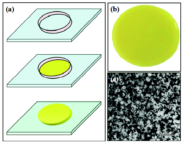
图1给出了制备荧光膜的流程图、实物图和光学显微照片。先在玻璃板上固定一层塑料圆形模具(可更换不同形状), 膜的形状和横截面积固定, 再置入定量的胶粉混合液, 在70-90℃烘烤40-100 min后剥离模具, 得到图1(b)中的荧光膜。图1(b)、(c)表明, 荧光膜表面光滑、无气泡孔, 荧光粉在硅胶中分散均匀, 且由于充分混合的荧光胶在模具槽内自由扩散, 荧光粉没有明显的的团聚、沉降以及膜凹凸不平。
图1 荧光膜的合成工艺、实物和微观结构影像图
Fig.1 Preparation process (a), photograph (b) and micrograph (c) of the fluorescent films
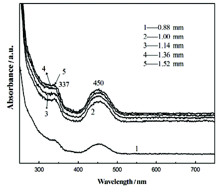
图2给出了将Y3Al5O12: Ce3+ (YAG)荧光粉与硅胶混合制备出的形状一致、不同厚度的荧光膜的吸收光谱图。图中位于337 nm和450 nm左右两个较宽的吸收峰属于YAG 荧光粉中Ce3+离子的f-d跃迁吸收, 且所有样品的谱线形状基本相同, 说明硅胶对Ce3+的吸收没有影响 [10, 13-15]。对比5个样品的吸收峰强度值可见, 随着荧光膜厚度的增大337 nm和450 nm的吸收强度提高, 特别是当厚度从0.88 mm到1.00 mm时, 荧光膜的吸收度增加幅度大, 因为YAG荧光粉的比例增大。而当荧光膜厚度大于1.00 mm, 特别是当荧光膜厚度为1.14 mm时, 荧光膜吸收度的提高非常缓慢, 几乎不再变化, 表明此时样品在337 nm和450 nm的吸收几乎达到饱和。
图2 不同厚度荧光膜的紫外-可见吸收光谱图
Fig.2 UV-Vis absorption spectra of the YAG fluorescent films with different thickness
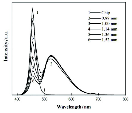
图3给出了采用荧光膜封装的模组白光LED的电致发射光谱图(驱动电流300 mA)。图中曲线1为芯片的发射光谱, 峰值波长位于455 nm处; 样品2-5的光谱形状、波峰位置均不变, 分别位于455 和525 nm。随着荧光膜厚度的增大, Ga(In)N模组位于455 nm左右的发射强度依次降低, 因为YAG荧光粉中Ce3+的f-d跃迁吸收芯片模组位于455 nm左右的蓝光波段。荧光膜厚度的增大, 荧光粉的质量和膜的厚度也增大, 使芯片发出的蓝光透过率降低, 其强度逐渐降低。而位于525 nm左右的黄光部分发射强度在荧光膜厚度为0.88 mm时最低, 其它厚度时基本保持不变。位于525 nm的黄光部分是YAG荧光粉受芯片激发发出的光[13-15]。从图2可见, 当荧光膜厚度超过1 mm后蓝光的吸收度变化不大, 芯片蓝光激发的525 nm 左右的发射光谱也几乎重合, 荧光粉发光强度几乎保持不变。因此图2和图3表明, 荧光膜的厚度对白光LED器件的性能有较大影响, 当其厚度为1.00 mm 时荧光膜厚度比较合适, 得到的LED器件发光强度高。
图3 基于蓝光LED模组和不同厚度荧光膜封装的LED器件的电致发射光谱(IF = 300 mA)
Fig.3 Electroluminescence spectra of the fabricated LEDs based on blue LED modules and fluorescent films (IF = 300 mA)
表1给出了从图3的电致光谱中测试白光LED灯的光学参数。表1的结果表明:调整荧光膜的厚度可得到色温从4700到6700 K的白光LED器件。但是0.88 mm荧光膜封器件的光效最低, 为69.89 lm/W, 1.00 mm荧光膜封装器件的光效增加到76.35 lm/W, 而对于厚度大于1.00 mm的荧光膜封装器件光效变化不大, 基本都为77 lm/W, 这主要是因为对光通量贡献最大的525 nm左右发射光谱强度基本相同造成的。同时, 白光LED显色指数从72.4降低到61.2。与0.88 mm样品相比, LED器件显色指数低, 但在光效上提高10%左右; 与大于1.00 mm的样品相比, 显色指数高, 光效比较接近。可见, 荧光膜厚度为1.00 mm的封装得到的白光LED器件性能较好。
表1 基于蓝光LED模组和不同厚度荧光膜封装的LED器件的光色参数(IF = 300 mA)
Table 1 Parameters of the fabricated LEDs based on blue LED modules and fluorescent films (IF = 300 mA)
| Thickness(mm) | Luminous efficiency (lm/W) | x | y | Tc(K) | Ra |
|---|---|---|---|---|---|
| 0.88 | 69.89 | 0.3034 | 0.359 | 6737 | 72.4 |
| 1.00 | 76.35 | 0.3277 | 0.4066 | 5660 | 67.7 |
| 1.14 | 76.96 | 0.3457 | 0.4416 | 5184 | 64.9 |
| 1.36 | 76.28 | 0.3602 | 0.4691 | 4902 | 62.7 |
| 1.52 | 77.79 | 0.3695 | 0.4864 | 4752 | 61.2 |
图4(a)给出了用1.02 mm橙色Sr3SiO5:Eu2+荧光膜与约455 nm 蓝光Ga(In)N芯片模组封装的LED灯的电致发射光谱(9 V, 300 mA))。约455 nm左右蓝光来自Ga(In)N芯片的电致发射光, 位于575 nm的发射峰为是Sr3SiO5:Eu2+荧光粉被蓝光LED激发后Eu2+的f-d跃迁发射[16-17], 所得到白光LED器件相关色温约为4450 K, 光效约为76.5 lm/W, 显色指数为73.7, CIE色坐标值分别为(0.3617, 0.3627), 接近普朗克轨迹线, 如图4(b)1931年色坐标图所示[18-19]。这些实验结果表明, 封装的白光LED模组可用于室内照明, 提高通用照明的光色质量。
图4 用蓝光芯片和Sr3SiO5:Eu2+荧光膜封装的(a)电致发射光谱图; (b)1931 CIE色坐标图(IF = 300 mA)
Fig.4 Electroluminescence spectra of LEDs (a); CIE 1931 chromaticity diagram based on blue LED modules and Sr3SiO5:Eu2+ fluorescent films (IF = 300 mA) (b)
显色指数是还原物体颜色真实程度的标准, 按照标准的计算方法, 一定的红光引入可提高YAG类荧光粉转换白光LED的显色指数[4]。图5给出了使用一定比例的YAG黄色荧光粉和Sr2Si5N8:Eu2+红色荧光粉和硅胶制备的1.00 mm荧光膜与模组封装的白光LED的电致发射光谱(IF = 300 mA)。从图5可见, 与YAG荧光膜封装器件相比, Sr2Si5N8:Eu2+红色荧光粉的加入使得器件在640 nm左右出现一个强的发射峰, 所封装的白光LED色温约为2700 K, 光效约为52.6 lm/W, 显色指数可达到91.7。这个结果表明, 引入适当强度的红光可提高LED的显色指数。
图5 封装的高显色指数LED器件的电致发射光谱图(IF = 300 mA)
Fig.5 Electroluminescence spectra of the high rendering index LEDs (IF = 300 mA)
使用荧光粉和硅胶可制备出荧光粉均匀分散、表面平整的荧光膜, 与455 nm蓝光芯片模组组装成高功率的白光LED器件。Y3Al5O12: Ce3+ (YAG)荧光膜的吸收光谱峰分别位于337 nm和450 nm左右, 与YAG荧光粉中Ce3+的f-d跃迁吸收对应, 且当荧光膜厚度为1.00 mm时制备出的功率为2.8 W左右的LED模组光色参数较好。将不同比例红色荧光粉和黄色荧光粉按上述厚度和条件可制备出高显色荧光膜和低色温4460 K、高显色指数91.7的白光LED器件。
The authors have declared that no competing interests exist.
| [1] |
High-power phosphor-converted light-emitting diodes based on III-nitrides , |
| [2] |
Recent results on the degradation of white LEDs for lighting ,
|
| [3] |
Excellent color rendering indexes of multi-package white LEDs ,
|
| [4] |
|
| [5] |
Progress in research on silicon-nitride based phosphor for white LED ,
白光LED用硅氮基荧光粉材料研究进展 ,
|
| [6] |
Analysis of DC current accelerated life tests of GaN LEDs using a Weibull-based statistical model, IEEE Transactions on , |
| [7] |
The study on the effect of the relative position of the phosphor layer in the LED package on the high power LED lifetime ,
|
| [8] |
The impact of inhomogeneities in the phosphor distribution on the device performance of phosphor-converted high-power white LED light sources , |
| [9] |
High Efficiency GaN-based High-voltage Light-emitting Diode Chips and Its Chip-on-board Packaging ,高效率GaN基高压LED芯片的制备及COB封装 , |
| [10] |
Thermally Activated Degradation of Remote Phosphors for Application in LED Lighting, IEEE Transactions on , |
| [11] |
Luminescence and scintillation properties of YAG:Ce single crystal and optical ceramics , |
| [12] |
YAG glass-ceramic phosphor for white LED (I): background and development, Optics & Photonics2005 ,
|
| [13] |
Properties of transparent Ce:YAG ceramic phosphors for white LED ,
<h2 class="secHeading" id="section_abstract">Abstract</h2><p id="sp005">Transparent Ce:YAG ceramic phosphors were synthesized from the oxide powder which was produced by co-preparation method of the hydroxides. The Ce:YAG ceramics had a broad emission band peaked at 530 nm due to the 5d → 4f transition of Ce<sup>3+</sup>. The transmittances of the samples obtained were 70–87% at 800 nm. The absorption coefficient and emission intensity of Ce<sup>3+</sup> were increased with increasing thickness. Under 465 nm LED excitation, the color coordinates of the Ce:YAG ceramics shifted from the blue region to yellow region with increasing sample thickness, passing nearby the theoretical white point in the chromaticity diagram. The highest value of luminous efficacy of the ceramic white LED was 73.5 lm/W.</p>
|
| [14] |
Properties of transparent Ce: YAG ceramic phosphors for white LED ,
|
| [15] |
Synthesis and Properties of Well-dispersive and Spherical YAG:Ce3+ Phosphors ,易分散球形YAG:Ce3+荧光粉的制备和性能 ,
将微波均相沉淀与喷雾干燥相结合, 并添加助熔剂辅助煅烧制备出单相YAG:Ce3+荧光粉体, 研究了微波均相沉淀与喷雾干燥的共同作用对煅烧条件和YAG:Ce3+荧光粉颗粒形貌、分散性和荧光性能的影响。结果表明, 这种单相YAG:Ce3+荧光粉体具有良好分散性, 平均粒径为2 μm; 将微波均相沉淀与喷雾干燥相结合能制备出分散性好的球形YAG前驱体颗粒; 添加NaF助熔剂使煅烧温度降低至1150℃, 并得到纯YAG晶相;随着NaF添加量的增加荧光粉结晶度提高、发光强度增强、发射光谱蓝移;NaF添加量(质量分数)为6%时荧光粉的荧光强度最高, 且与单一助熔剂比较, H3BO3--NaF混合助熔剂能更好的改善YAG:Ce3+的荧光性能。
|
| [16] |
Preparation and luminescence characteristics of Sr3SiO5: Eu2+ phosphor for white LED , |
| [17] |
Synthesis, Persistent Luminescence, and Thermoluminescence Properties of Yellow Sr3SiO5: Eu2+, RE3+(RE= Ce, Nd, Dy, Ho, Er, Tm, Yb) and Orange-Red Sr3-xBaxSiO5: Eu2+, Dy3+ Phosphor , |
| [18] |
White thin-film flip-chip LEDs with uniform color temperature using laser lift-off and conformal phosphor coating technologies , |
| [19] |
|

/
| 〈 |
|
〉 |

